- 您现在的位置:买卖IC网 > PDF目录1832 > LTC3833EFE#PBF (Linear Technology)IC REG CTRLR BUCK PWM CM 20TSSOP PDF资料下载
参数资料
| 型号: | LTC3833EFE#PBF |
| 厂商: | Linear Technology |
| 文件页数: | 13/36页 |
| 文件大小: | 0K |
| 描述: | IC REG CTRLR BUCK PWM CM 20TSSOP |
| 标准包装: | 74 |
| PWM 型: | 电流模式 |
| 输出数: | 1 |
| 频率 - 最大: | 2.2MHz |
| 电源电压: | 4.5 V ~ 38 V |
| 降压: | 是 |
| 升压: | 无 |
| 回扫: | 无 |
| 反相: | 无 |
| 倍增器: | 无 |
| 除法器: | 无 |
| Cuk: | 无 |
| 隔离: | 无 |
| 工作温度: | -40°C ~ 125°C |
| 封装/外壳: | 20-TSSOP(0.173",4.40mm 宽)裸露焊盘 |
| 包装: | 管件 |
第1页第2页第3页第4页第5页第6页第7页第8页第9页第10页第11页第12页当前第13页第14页第15页第16页第17页第18页第19页第20页第21页第22页第23页第24页第25页第26页第27页第28页第29页第30页第31页第32页第33页第34页第35页第36页
�� �
�
�LTC3833�
�APPLICATIONS� INFORMATION�
�The� Typical� Application� on� the� first� page� of� this� data� sheet�
�is� a� basic� LTC3833� application� circuit.� The� LTC3833� can� be�
�configured� to� sense� the� inductor� current� either� through� a�
�series� sense� resistor,� R� SENSE� ,� or� through� an� RC� filter� across�
�the� inductor� (DCR).� The� choice� between� the� two� current�
�sensing� schemes� is� largely� a� design� trade-off� between�
�cost,� power� consumption� and� accuracy.� DCR� sensing�
�is� becoming� popular� because� it� saves� expensive� current�
�sensing� resistors� and� is� more� power� efficient,� especially�
�in� high� current� applications.� However,� current� sensing�
�resistors� provide� the� most� accurate� current� limits� for� the�
�controller.� Once� the� required� output� voltage� and� operat-�
�ing� frequency� have� been� determined,� external� component�
�selection� is� driven� by� load� requirements,� and� begins� with�
�the� selection� of� inductor� and� current� sensing� components.�
�Next,� the� power� MOSFETs� are� selected.� Finally,� input� and�
�output� capacitors� are� selected.�
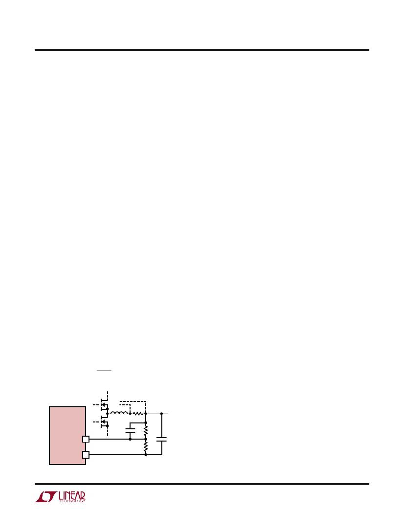
�Output� Voltage� Programming� and�
�Differential� Output� Sensing�
�The� LTC3833� integrates� differential� output� sensing� with�
�output� voltage� programming,� allowing� for� simple� and�
�seamless� design.� As� shown� in� Figure� 1,� the� output� voltage�
�is� programmed� by� an� external� resistor� divider� from� the�
�regulated� output� point� to� its� ground� reference.� The� resis-�
�tive� divider� is� tapped� by� the� V� OSNS+� pin,� and� the� ground�
�reference� is� sensed� by� V� OSNS–� .� An� optional� feed-forward�
�capacitor,� C� FF� ,� can� be� used� to� improve� the� transient�
�performance� of� the� regulator� system� as� discussed� under�
�OPTI-LOOP� ?� Compensation.� The� resulting� output� voltage�
�is� given� according� to� the� following� equation:�
�More� precisely,� the� V� OUT� value� programmed� in� the� previous�
�equation� is� with� respect� to� the� output’s� ground� reference,�
�and� thus� is� a� differential� quantity.� For� example,� if� V� OUT� is�
�programmed� to� 5V� and� the� output� ground� reference� is� at�
�–0.5V,� then� the� output� will� be� 4.5V� with� respect� to� signal�
�ground.� The� minimum� differential� output� voltage� is� limited�
�to� the� internal� reference,� 0.6V,� and� the� maximum� differential�
�output� voltage� is� 5.5V.�
�The� V� OSNS+� pin� is� high� impedance� with� no� input� bias� cur-�
�rent.� The� V� OSNS–� pin� has� about� 35μA� of� current� flowing�
�out� of� the� pin.�
�Differential� output� sensing� allows� for� more� accurate� output�
�regulation� in� high� power� distributed� systems� having� large�
�line� losses.� Figure� 2� illustrates� the� potential� variations� in�
�the� power� and� ground� lines� due� to� parasitic� elements.�
�These� variations� are� exacerbated� in� multi-application�
�systems� with� shared� ground� planes.� Without� differential�
�output� sensing,� these� variations� directly� reflect� as� an� error�
�in� the� regulated� output� voltage.� The� LTC3833’s� differential�
�output� sensing� can� correct� for� up� to� ±500mV� of� variation�
�in� the� output’s� power� and� ground� lines.�
�The� LTC3833’s� differential� output� sensing� scheme� is�
�distinct� from� conventional� schemes� where� the� regulated�
�output� and� its� ground� reference� are� directly� sensed� with�
�a� difference� amplifier� whose� output� is� then� divided� down�
�with� an� external� resistive� divider� and� fed� into� the� error�
�amplifier� input.� This� conventional� scheme� is� limited� by�
�the� common� mode� input� range� of� the� difference� amplifier�
�and� typically� limits� differential� sensing� to� the� lower� range�
�of� output� voltages.�
�V� OUT� =� 0.6V� ?� ?� 1� +� FB2� ?�
�C� FF�
�R� FB2�
�?� R� ?�
�?� R� FB1� ?�
�LTC3833�
�(OPT)�
�V� OSNS+�
�R� FB1�
�V� OSNS–�
�Figure� 1.� Setting� Output� Voltage�
�V� OUT�
�C� OUT�
�3833� F01�
�The� LTC3833� allows� for� seamless� differential� output�
�sensing� by� sensing� the� resistively� divided� feedback� volt-�
�age� differentially.� This� allows� for� differential� sensing� in�
�the� full� output� range� from� 0.6V� to� 5.5V.� The� difference�
�amplifier� of� the� LTC3833� has� a� –3dB� bandwidth� of� 8MHz,�
�high� enough� to� not� affect� main� loop� compensation� and�
�transient� behavior.�
�To� avoid� noise� coupling� into� V� OSNS+� ,� the� resistor� divider�
�should� be� placed� near� the� V� OSNS+� and� V� OSNS–� pins� and�
�physically� close� to� the� LTC3833.� The� remote� output� and�
�ground� traces� should� be� routed� together� as� a� differential�
�pair� to� the� remote� output.� These� traces� should� be� termi-�
�nated� as� close� as� physically� possible� to� the� remote� output�
�3833f�
�13�
�相关PDF资料 |
PDF描述 |
|---|---|
| LTC3834EFE#PBF | IC REG CTRLR BUCK PWM CM 20TSSOP |
| LTC3835IFE#PBF | IC REG CTRLR BUCK PWM CM 20TSSOP |
| LTC3836EUFD#TRPBF | IC REG CTRLR BUCK PWM CM 28-QFN |
| LTC3838IFE#TRPBF | IC REG CTRLR BUCK PWM CM 38TSSOP |
| LTC3839EUH#PBF | IC REG CTRLR BUCK PWM CM 32-QFN |
相关代理商/技术参数 |
参数描述 |
|---|---|
| LTC3833EUDC#PBF | 功能描述:IC REG CTRLR BUCK PWM CM 20-QFN RoHS:是 类别:集成电路 (IC) >> PMIC - 稳压器 - DC DC 切换控制器 系列:- 标准包装:2,500 系列:- PWM 型:电流模式 输出数:1 频率 - 最大:500kHz 占空比:96% 电源电压:4 V ~ 36 V 降压:无 升压:是 回扫:无 反相:无 倍增器:无 除法器:无 Cuk:无 隔离:无 工作温度:-40°C ~ 125°C 封装/外壳:24-WQFN 裸露焊盘 包装:带卷 (TR) |
| LTC3833EUDC#TRPBF | 功能描述:IC REG CTRLR BUCK PWM CM 20-QFN RoHS:是 类别:集成电路 (IC) >> PMIC - 稳压器 - DC DC 切换控制器 系列:- 标准包装:2,500 系列:- PWM 型:电流模式 输出数:1 频率 - 最大:500kHz 占空比:96% 电源电压:4 V ~ 36 V 降压:无 升压:是 回扫:无 反相:无 倍增器:无 除法器:无 Cuk:无 隔离:无 工作温度:-40°C ~ 125°C 封装/外壳:24-WQFN 裸露焊盘 包装:带卷 (TR) |
| LTC3833IFE#PBF | 功能描述:IC REG CTRLR BUCK PWM CM 20TSSOP RoHS:是 类别:集成电路 (IC) >> PMIC - 稳压器 - DC DC 切换控制器 系列:- 标准包装:2,500 系列:- PWM 型:电流模式 输出数:1 频率 - 最大:500kHz 占空比:96% 电源电压:4 V ~ 36 V 降压:无 升压:是 回扫:无 反相:无 倍增器:无 除法器:无 Cuk:无 隔离:无 工作温度:-40°C ~ 125°C 封装/外壳:24-WQFN 裸露焊盘 包装:带卷 (TR) |
| LTC3833IFE#TRPBF | 功能描述:IC REG CTRLR BUCK PWM CM 20TSSOP RoHS:是 类别:集成电路 (IC) >> PMIC - 稳压器 - DC DC 切换控制器 系列:- 标准包装:2,500 系列:- PWM 型:电流模式 输出数:1 频率 - 最大:500kHz 占空比:96% 电源电压:4 V ~ 36 V 降压:无 升压:是 回扫:无 反相:无 倍增器:无 除法器:无 Cuk:无 隔离:无 工作温度:-40°C ~ 125°C 封装/外壳:24-WQFN 裸露焊盘 包装:带卷 (TR) |
| LTC3833IUDC#PBF | 功能描述:IC REG CTRLR BUCK PWM CM 20-QFN RoHS:是 类别:集成电路 (IC) >> PMIC - 稳压器 - DC DC 切换控制器 系列:- 标准包装:2,500 系列:- PWM 型:电流模式 输出数:1 频率 - 最大:500kHz 占空比:96% 电源电压:4 V ~ 36 V 降压:无 升压:是 回扫:无 反相:无 倍增器:无 除法器:无 Cuk:无 隔离:无 工作温度:-40°C ~ 125°C 封装/外壳:24-WQFN 裸露焊盘 包装:带卷 (TR) |
发布紧急采购,3分钟左右您将得到回复。