- 您现在的位置:买卖IC网 > PDF目录79926 > LTC3872ETS8#PBF (LINEAR TECHNOLOGY CORP) SWITCHING CONTROLLER, 650 kHz SWITCHING FREQ-MAX, PDSO8 PDF资料下载
参数资料
| 型号: | LTC3872ETS8#PBF |
| 厂商: | LINEAR TECHNOLOGY CORP |
| 元件分类: | 稳压器 |
| 英文描述: | SWITCHING CONTROLLER, 650 kHz SWITCHING FREQ-MAX, PDSO8 |
| 封装: | 1 MM HEIGHT, LEAD FREE, PLASTIC, MO-193, TSOT-23, 8 PIN |
| 文件页数: | 7/22页 |
| 文件大小: | 245K |
| 代理商: | LTC3872ETS8#PBF |
LTC3872
15
3872fb
And so the inductor value is:
L
=
VIN(MIN)
IL f
DMAX =
3.3V
1.3A 550kHz
0.39
= 1.8H
The component chosen is a 2.2H inductor made by
Sumida (part number CEP125-H 1ROMH).
3. Assuming a MOSFET junction temperature of 125°C,
the room temperature MOSFET RDS(ON) should be less
than:
RDS(ON) ≤ VSENSE(MAX)
1– DMAX
1
+ χ
2
IO(MAX) ρT
= 0.175V
1– 0.39
1
+
0.4
2
2A 1.5
≈ 30m
The MOSFET used was the Si3460, which has a maximum
RDS(ON) of 27mΩ at 4.5V VGS, a BVDSS of greater than
30V, and a gate charge of 13.5nC at 4.5V VGS.
4. The diode for this design must handle a maximum DC
output current of 2A and be rated for a minimum reverse
voltage of VOUT, or 5V. A 25A, 15V diode from On Semi-
conductor (MBRB2515L) was chosen for its high power
dissipation capability.
5. The output capacitor usually consists of a lower valued,
low ESR ceramic.
6. The choice of an input capacitor for a boost converter
depends on the impedance of the source supply and the
amount of input ripple the converter will safely tolerate.
For this particular design two 22F Taiyo Yuden ceramic
capacitors (JMK325BJ226MM) is required (the input
and return lead lengths are kept to a few inches. As with
the output node, check the input ripple with a single
oscilloscope probe connected across the input capacitor
terminals.
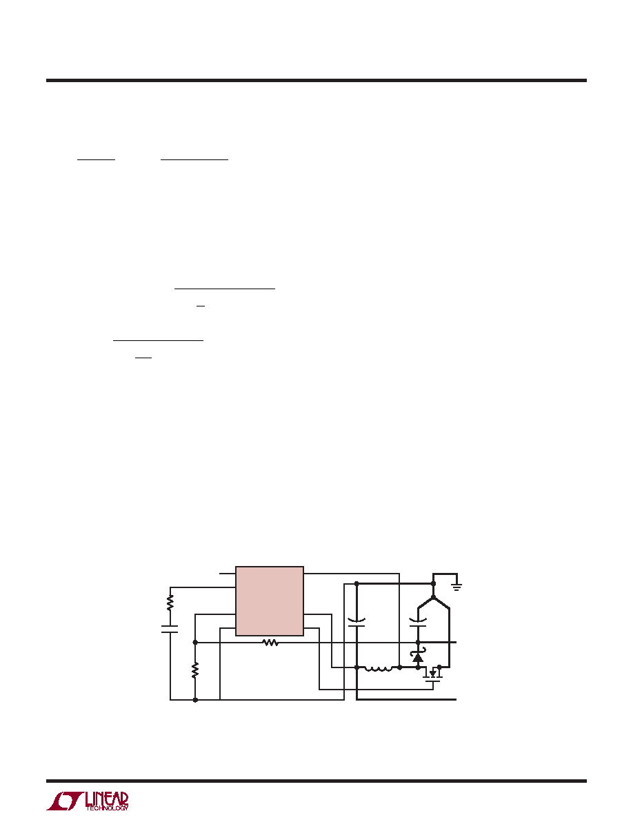
PC Board Layout Checklist
When laying out the printed circuit board, the following
checklist should be used to ensure proper operation of
the LTC3872. These items are illustrated graphically in
the layout diagram in Figure 8. Check the following in
your layout:
1. TheSchottkydiodeshouldbecloselyconnectedbetween
the output capacitor and the drain of the external MOSFET.
2. The input decoupling capacitor (0.1F) should be con-
nected closely between VIN and GND.
3. The trace from SW to the switch point should be kept
short.
4. Keep the switching node NGATE away from sensitive
small signal nodes.
5. The VFB pin should connect directly to the feedback
resistors. The resistive divider R1 and R2 must be con-
nected between the (+) plate of COUT and signal ground.
Figure 8. LTC3872 Layout Diagram (See PC Board Layout Checklist)
IPRG
ITH
VFB
GND
SW
RUN/SS
VIN
NGATE
LTC3872
3872 F08
R1
R2
RITH
CIN
COUT
VOUT
VIN
CITH
+
D1
M1
L1
BOLD LINES INDICATE HIGH CURRENT PATHS
applicaTions inForMaTion
相关PDF资料 |
PDF描述 |
|---|---|
| LTC3850EGN | 0.1 A DUAL SWITCHING CONTROLLER, 860 kHz SWITCHING FREQ-MAX, PDSO28 |
| LT1933HS6#TR | 1.05 A SWITCHING REGULATOR, 600 kHz SWITCHING FREQ-MAX, PDSO6 |
| LC016AJ | 2-OUTPUT 16 W DC-DC REG PWR SUPPLY MODULE |
| LTC4224CMS-2#PBF | 2-CHANNEL POWER SUPPLY SUPPORT CKT, PDSO10 |
| LTC4224IMS-1#PBF | 2-CHANNEL POWER SUPPLY SUPPORT CKT, PDSO10 |
相关代理商/技术参数 |
参数描述 |
|---|---|
| LTC3872HDDB#TRMPBF | 功能描述:IC REG CTRLR BST PWM CM 8-DFN RoHS:是 类别:集成电路 (IC) >> PMIC - 稳压器 - DC DC 切换控制器 系列:- 标准包装:2,500 系列:- PWM 型:电流模式 输出数:1 频率 - 最大:500kHz 占空比:96% 电源电压:4 V ~ 36 V 降压:无 升压:是 回扫:无 反相:无 倍增器:无 除法器:无 Cuk:无 隔离:无 工作温度:-40°C ~ 125°C 封装/外壳:24-WQFN 裸露焊盘 包装:带卷 (TR) |
| LTC3872HDDB#TRPBF | 功能描述:IC REG CTRLR BST PWM CM 8-DFN RoHS:是 类别:集成电路 (IC) >> PMIC - 稳压器 - DC DC 切换控制器 系列:- 标准包装:2,500 系列:- PWM 型:电流模式 输出数:1 频率 - 最大:500kHz 占空比:96% 电源电压:4 V ~ 36 V 降压:无 升压:是 回扫:无 反相:无 倍增器:无 除法器:无 Cuk:无 隔离:无 工作温度:-40°C ~ 125°C 封装/外壳:24-WQFN 裸露焊盘 包装:带卷 (TR) |
| LTC3872HTS8#PBF | 制造商:Linear Technology 功能描述:DP-SWREG/Controller, CUT TAPE No Rsense, Current Mode Boost DC/DC Controller |
| LTC3872HTS8#TRMPBF | 功能描述:IC REG CTRLR BST PWM CM TSOT23-8 RoHS:是 类别:集成电路 (IC) >> PMIC - 稳压器 - DC DC 切换控制器 系列:- 标准包装:2,500 系列:- PWM 型:电流模式 输出数:1 频率 - 最大:500kHz 占空比:96% 电源电压:4 V ~ 36 V 降压:无 升压:是 回扫:无 反相:无 倍增器:无 除法器:无 Cuk:无 隔离:无 工作温度:-40°C ~ 125°C 封装/外壳:24-WQFN 裸露焊盘 包装:带卷 (TR) |
| LTC3872HTS8#TRPBF | 功能描述:IC REG CTRLR BST PWM CM TSOT23-8 RoHS:是 类别:集成电路 (IC) >> PMIC - 稳压器 - DC DC 切换控制器 系列:- 标准包装:2,500 系列:- PWM 型:电流模式 输出数:1 频率 - 最大:500kHz 占空比:96% 电源电压:4 V ~ 36 V 降压:无 升压:是 回扫:无 反相:无 倍增器:无 除法器:无 Cuk:无 隔离:无 工作温度:-40°C ~ 125°C 封装/外壳:24-WQFN 裸露焊盘 包装:带卷 (TR) |
发布紧急采购,3分钟左右您将得到回复。