- 您现在的位置:买卖IC网 > PDF目录79821 > LTC3890IUH#PBF (LINEAR TECHNOLOGY CORP) DUAL SWITCHING CONTROLLER, 585 kHz SWITCHING FREQ-MAX, PQCC32 PDF资料下载
参数资料
| 型号: | LTC3890IUH#PBF |
| 厂商: | LINEAR TECHNOLOGY CORP |
| 元件分类: | 稳压器 |
| 英文描述: | DUAL SWITCHING CONTROLLER, 585 kHz SWITCHING FREQ-MAX, PQCC32 |
| 封装: | 5 X 5 MM, 0.75 MM HEIGHT, LEAD FREE, PLASTIC, MO-220WHHD, QFN-32 |
| 文件页数: | 15/38页 |
| 文件大小: | 381K |
| 代理商: | LTC3890IUH#PBF |
第1页第2页第3页第4页第5页第6页第7页第8页第9页第10页第11页第12页第13页第14页当前第15页第16页第17页第18页第19页第20页第21页第22页第23页第24页第25页第26页第27页第28页第29页第30页第31页第32页第33页第34页第35页第36页第37页第38页
LTC3890
22
3890fa
EXTVCC
VIN
TG1
SW
BG1
PGND
1/2 LTC3890
RSENSE
VOUT
NDS7002
COUT
3890 F09
MBOT
MTOP
CIN
L
BAT85
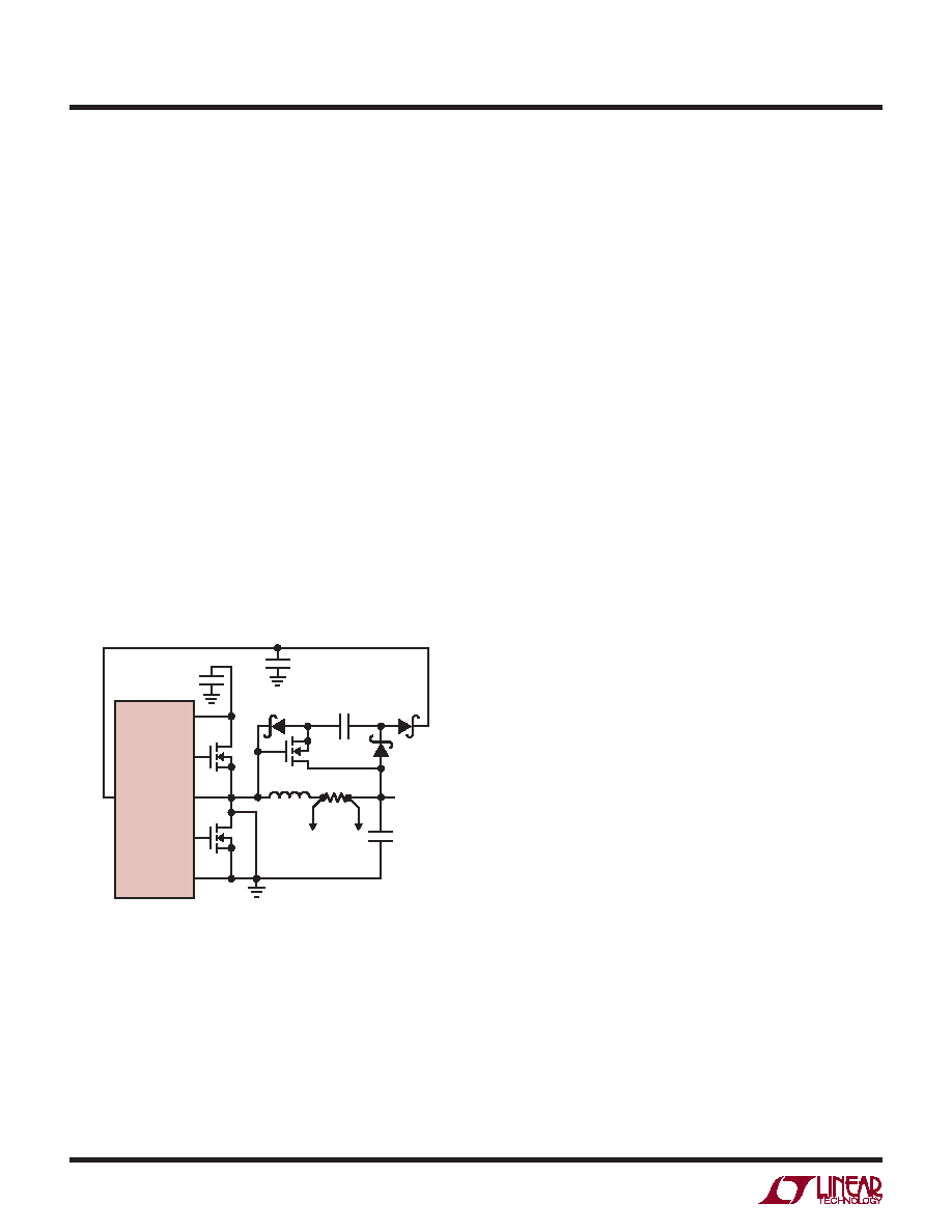
Figure 9. Capacitive Charge Pump for EXTVCC
The following list summarizes the four possible connec-
tions for EXTVCC:
1. EXTVCC Grounded.ThiswillcauseINTVCCtobepowered
from the internal 5.1V regulator resulting in an efficiency
penalty of up to 10% at high input voltages.
2. EXTVCC Connected Directly to VOUT. This is the normal
connection for a 5V to 14V regulator and provides the
highest efficiency.
3. EXTVCC Connected to an External Supply. If an external
supply is available in the 5V to 14V range, it may be
used to power EXTVCCprovidingitiscompatiblewiththe
MOSFET gate drive requirements. Ensure that EXTVCC
< VIN.
4. EXTVCCConnectedtoanOutput-DerivedBoostNetwork.
For 3.3V and other low voltage regulators, efficiency
gains can still be realized by connecting EXTVCC to an
output-derived voltage that has been boosted to greater
than 4.7V. This can be done with the capacitive charge
pump shown in Figure 9. Ensure that EXTVCC < VIN.
APPLICATIONS INFORMATION
desired MOSFET. This enhances the top MOSFET switch
and turns it on. The switch node voltage, SW, rises to VIN
and the BOOST pin follows. With the topside MOSFET
on, the boost voltage is above the input supply: VBOOST =
VIN + VINTVCC. The value of the boost capacitor, CB, needs
to be 100 times that of the total input capacitance of the
topside MOSFET(s). The reverse breakdown of the external
Schottky diode must be greater than VIN(MAX).
The external diode DB can be a Schottky diode or silicon
diode, but in either case it should have low-leakage and
fast recovery. Pay close attention to the reverse leakage
current specification for this diode, especially at high
temperatures where it generally increases substantially.
For applications with output voltages greater than ~5V
that are switching infrequently, a leaky diode DB can fully
discharge the bootstrap capacitor CB, creating a current
path from the output voltage to the BOOST pin to INTVCC.
Not only does this increase the quiescent current of the
converter, but it can cause INTVCC to rise to dangerous
levels if the leakage exceeds the current consumption on
INTVCC.
Particularly, this is a concern in Burst Mode operation at
no load or very light loads, where the part is switching
very infrequently and the current draw on INTVCC is very
low (typically about 35μA). Generally, pulse-skipping and
forced continuous modes are less sensitive to leakage,
since the more frequent switching keeps the bootstrap
capacitor CB charged, preventing a current path from the
output voltage to INTVCC.
However, in cases where the converter has been operat-
ing (in any mode) and then is shut down, if the leakage
of diode DB fully discharges the bootstrap capacitor CB
before the output voltage discharges to below ~5V, then
the leakage current path can be created from the output
voltage to INTVCC. In shutdown, the INTVCC pin is able to
sink about 30μA. To accommodate diode leakage greater
than this amount in shutdown, INTVCC can be loaded
with an external resistor or clamped with a Zener diode.
Alternatively, the PGOOD resistor can be used to sink the
current (assuming the resistor pulls up to INTVCC) since
PGOOD is pulled low when the converter is shut down.
Nonetheless, using a low-leakage diode is the best choice
to maintain low quiescent current under all conditions.
Topside MOSFET Driver Supply (CB, DB)
External bootstrap capacitors, CB, connected to the BOOST
pins supply the gate drive voltages for the topside MOSFETs.
Capacitor CB in the Functional Diagram is charged though
external diode DB from INTVCC when the SW pin is low.
When one of the topside MOSFETs is to be turned on, the
driver places the CB voltage across the gate-source of the
相关PDF资料 |
PDF描述 |
|---|---|
| LTC3615IFE-1#TRPBF | SWITCHING REGULATOR, PDSO24 |
| LTC3529EDCB#TRMPBF | SWITCHING CONTROLLER, 1800 kHz SWITCHING FREQ-MAX, PDSO8 |
| LM1001-7ERV0H | 1-OUTPUT 50 W AC-DC REG PWR SUPPLY MODULE |
| LM1001-7ERV3AF | 1-OUTPUT 50 W AC-DC REG PWR SUPPLY MODULE |
| LM1001-7PD4 | 1-OUTPUT 50 W AC-DC REG PWR SUPPLY MODULE |
相关代理商/技术参数 |
参数描述 |
|---|---|
| LTC3890MPGN-1#PBF | 功能描述:IC REG CTRLR BUCK PWM CM 28-SSOP RoHS:是 类别:集成电路 (IC) >> PMIC - 稳压器 - DC DC 切换控制器 系列:PolyPhase® 标准包装:4,500 系列:PowerWise® PWM 型:控制器 输出数:1 频率 - 最大:1MHz 占空比:95% 电源电压:2.8 V ~ 5.5 V 降压:是 升压:无 回扫:无 反相:无 倍增器:无 除法器:无 Cuk:无 隔离:无 工作温度:-40°C ~ 125°C 封装/外壳:6-WDFN 裸露焊盘 包装:带卷 (TR) 配用:LM1771EVAL-ND - BOARD EVALUATION LM1771 其它名称:LM1771SSDX |
| LTC3890MPGN-1#TRPBF | 功能描述:IC REG CTRLR BUCK PWM CM 28-SSOP RoHS:是 类别:集成电路 (IC) >> PMIC - 稳压器 - DC DC 切换控制器 系列:PolyPhase® 标准包装:4,500 系列:PowerWise® PWM 型:控制器 输出数:1 频率 - 最大:1MHz 占空比:95% 电源电压:2.8 V ~ 5.5 V 降压:是 升压:无 回扫:无 反相:无 倍增器:无 除法器:无 Cuk:无 隔离:无 工作温度:-40°C ~ 125°C 封装/外壳:6-WDFN 裸露焊盘 包装:带卷 (TR) 配用:LM1771EVAL-ND - BOARD EVALUATION LM1771 其它名称:LM1771SSDX |
| LTC3890MPGN-3#PBF | 制造商:Linear Technology 功能描述:IC REG CTRLR BUCK PWM CM 28SSOP 制造商:Linear Technology 功能描述:DC-DC CONTROLLER BUCK 900KHZ 制造商:Linear Technology 功能描述:DC-DC CONTROLLER, BUCK, 900KHZ, SSOP-28 制造商:Linear Technology 功能描述:DC-DC CONTROLLER, BUCK, 900KHZ, SSOP-28; Primary Input Voltage:60V; No. of Outputs:2; No. of Pins:28; Operating Temperature Min:-55C; Operating Temperature Max:150C; Operating Temperature Range:-55C to +150C ;RoHS Compliant: Yes |
| LTC3890MPGN-3#TRPBF | 制造商:Linear Technology 功能描述:IC REG CTRLR BUCK PWM CM 28SSOP |
| LTC3890MPUH#PBF | 功能描述:IC REG CTRLR BUCK PWM CM 32-QFN RoHS:是 类别:集成电路 (IC) >> PMIC - 稳压器 - DC DC 切换控制器 系列:PolyPhase® 标准包装:4,500 系列:PowerWise® PWM 型:控制器 输出数:1 频率 - 最大:1MHz 占空比:95% 电源电压:2.8 V ~ 5.5 V 降压:是 升压:无 回扫:无 反相:无 倍增器:无 除法器:无 Cuk:无 隔离:无 工作温度:-40°C ~ 125°C 封装/外壳:6-WDFN 裸露焊盘 包装:带卷 (TR) 配用:LM1771EVAL-ND - BOARD EVALUATION LM1771 其它名称:LM1771SSDX |
发布紧急采购,3分钟左右您将得到回复。