- 您现在的位置:买卖IC网 > PDF目录15229 > LTC3891MPUDC#PBF (Linear Technology)IC REG CTRLR BUCK PWM CM 20-QFN PDF资料下载
参数资料
| 型号: | LTC3891MPUDC#PBF |
| 厂商: | Linear Technology |
| 文件页数: | 18/32页 |
| 文件大小: | 0K |
| 描述: | IC REG CTRLR BUCK PWM CM 20-QFN |
| 标准包装: | 91 |
| PWM 型: | 电流模式 |
| 输出数: | 1 |
| 频率 - 最大: | 835kHz |
| 占空比: | 99% |
| 电源电压: | 4 V ~ 60 V |
| 降压: | 是 |
| 升压: | 无 |
| 回扫: | 无 |
| 反相: | 无 |
| 倍增器: | 无 |
| 除法器: | 无 |
| Cuk: | 无 |
| 隔离: | 无 |
| 工作温度: | -55°C ~ 150°C |
| 封装/外壳: | 20-WFQFN 裸露焊盘 |
| 包装: | 管件 |
第1页第2页第3页第4页第5页第6页第7页第8页第9页第10页第11页第12页第13页第14页第15页第16页第17页当前第18页第19页第20页第21页第22页第23页第24页第25页第26页第27页第28页第29页第30页第31页第32页
�� �
�
�LTC3891�
�APPLICATIONS� INFORMATION�
�?� (� V� OUT� )� (� V� IN� –� V� OUT� )� ?�
�I� MAX� ?� ?� 1/2� (1)�
�C� IN� Required� I� RMS� ≈�
�1�
�Δ� V� OUT� ≈� Δ� I� L� ?� ESR� +� ?�
�maximumRMScurrentofonechannelmustbeused.The�
�maximum� RMS� capacitor� current� is� given� by:�
�V� IN�
�This� formula� has� a� maximum� at� V� IN� =� 2V� OUT� ,� where� I� RMS�
�=� I� OUT� /2.� This� simple� worst-case� condition� is� commonly�
�used� for� design� because� even� significant� deviations� do� not�
�offer� much� relief.� Note� that� capacitor� manufacturers’� ripple�
�current� ratings� are� often� based� on� only� 2000� hours� of� life.�
�This� makes� it� advisable� to� further� derate� the� capacitor,� or�
�to� choose� a� capacitor� rated� at� a� higher� temperature� than�
�required.� Several� capacitors� may� be� paralleled� to� meet�
�size� or� height� requirements� in� the� design.� Due� to� the� high�
�operating� frequency� of� the� LTC3891,� ceramic� capacitors�
�can� also� be� used� for� C� IN� .� Always� consult� the� manufacturer�
�if� there� is� any� question.�
�A� small� (0.1μF� to� 1μF)� bypass� capacitor� between� the� chip�
�V� IN� pin� and� ground,� placed� close� to� the� LTC3891,� is� also�
�suggested.� A� small� (≤10Ω)� resistor� placed� between� C� IN�
�(C1)� and� the� V� IN� pin� provides� further� isolation.�
�The� selection� of� C� OUT� is� driven� by� the� effective� series�
�resistance� (ESR).� Typically,� once� the� ESR� requirement�
�is� satisfied,� the� capacitance� is� adequate� for� filtering.� The�
�output� ripple� (?V� OUT� )� is� approximated� by:�
�?� ?�
�?� 8� ?� f� ?� C� OUT� ?�
�where� f� is� the� operating� frequency,� C� OUT� is� the� output�
�capacitance� and� ?I� L� is� the� ripple� current� in� the� inductor.�
�The� output� ripple� is� highest� at� maximum� input� voltage�
�since� ?I� L� increases� with� input� voltage.�
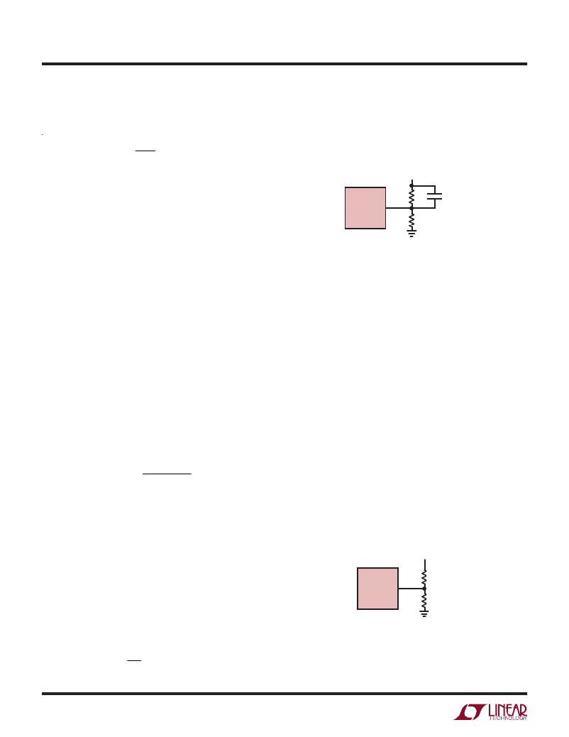
�To� improve� the� frequency� response,� a� feedforward� ca-�
�pacitor,� C� FF� ,� may� be� used.� Great� care� should� be� taken� to�
�route� the� V� FB� line� away� from� noise� sources,� such� as� the�
�inductor� or� the� SW� line.�
�V� OUT�
�LTC3891� R� B� C� FF�
�V� FB�
�R� A�
�3891� F03�
�Figure� 3.� Setting� Output� Voltage�
�RUN� Pin�
�The� LTC3891� is� enabled� using� the� RUN� pin.� It� has� a� rising�
�threshold� of� 1.21V� with� 50mV� of� hysteresis.� Pulling� the�
�RUN� pin� below� 1.16V� shuts� down� the� main� control� loop.�
�Pulling� it� below� 0.7V� disables� the� controller� and� most�
�internal� circuits,� including� the� INTV� CC� LDOs.� In� this� state,�
�the� LTC3891� draws� only� 14μA� of� quiescent� current.�
�Releasing� the� RUN� pin� allows� a� small� 7μA� internal� current�
�to� pull� up� the� pin� to� enable� the� controller.� The� RUN� pin� may�
�be� externally� pulled� up� or� driven� directly� by� logic.� When�
�driving� the� RUN� pin� with� a� low� impedance� source,� do� not�
�exceed� the� absolute� maximum� rating� of� 8V.� The� RUN� pin�
�has� an� internal� 11V� voltage� clamp� that� allows� the� RUN� pin�
�to� be� connected� through� a� resistor� to� a� higher� voltage� (for�
�example,� V� IN� ),� so� long� as� the� maximum� current� into� the�
�RUN� pin� does� not� exceed� 100μA.�
�The� RUN� pin� can� be� implemented� as� a� UVLO� by� connecting�
�it� to� the� output� of� an� external� resistor� divider� network� off�
�V� IN� ,� as� shown� in� Figure� 4.�
�V� IN�
�Setting� Output� Voltage�
�LTC3891�
�R� B�
�The� LTC3891� output� voltage� is� set� by� an� external� feed-�
�back� resistor� divider� carefully� placed� across� the� output,�
�as� shown� in� Figure� 3.� The� regulated� output� voltage� is�
�determined� by:�
�RUN�
�R� A�
�3891� F04�
�Figure� 4.� Using� the� RUN� Pin� as� a� UVLO�
�V� OUT� =� 0.8V� ?� 1� +� B� ?�
�?� R� ?�
�?� R� A� ?�
�3891fa�
�18�
�相关PDF资料 |
PDF描述 |
|---|---|
| RBM28DCMT | CONN EDGECARD 56POS .156 WW |
| GCM36DSXS | CONN EDGECARD 72POS DIP .156 SLD |
| NCP305LSQ20T1G | IC VOLT DETECT OD 2.0V SC-82AB |
| GCM28DSEI | CONN EDGECARD 56POS .156 EYELET |
| VE-JT3-EY-F4 | CONVERTER MOD DC/DC 24V 50W |
相关代理商/技术参数 |
参数描述 |
|---|---|
| LTC3900ES8 | 功能描述:IC DRIVER RECT SYNC CONV 8SOIC RoHS:否 类别:集成电路 (IC) >> PMIC - MOSFET,电桥驱动器 - 外部开关 系列:- 标准包装:5 系列:- 配置:低端 输入类型:非反相 延迟时间:600ns 电流 - 峰:12A 配置数:1 输出数:1 高端电压 - 最大(自引导启动):- 电源电压:14.2 V ~ 15.8 V 工作温度:-20°C ~ 60°C 安装类型:通孔 封装/外壳:21-SIP 模块 供应商设备封装:模块 包装:散装 配用:BG2A-NF-ND - KIT DEV BOARD FOR IGBT 其它名称:835-1063 |
| LTC3900ES8#PBF | 功能描述:IC DRIVER RECT SYNC CONV 8SOIC RoHS:是 类别:集成电路 (IC) >> PMIC - MOSFET,电桥驱动器 - 外部开关 系列:- 标准包装:5 系列:- 配置:低端 输入类型:非反相 延迟时间:600ns 电流 - 峰:12A 配置数:1 输出数:1 高端电压 - 最大(自引导启动):- 电源电压:14.2 V ~ 15.8 V 工作温度:-20°C ~ 60°C 安装类型:通孔 封装/外壳:21-SIP 模块 供应商设备封装:模块 包装:散装 配用:BG2A-NF-ND - KIT DEV BOARD FOR IGBT 其它名称:835-1063 |
| LTC3900ES8#TR | 功能描述:IC DRIVER RECT SYNC CONV 8SOIC RoHS:否 类别:集成电路 (IC) >> PMIC - MOSFET,电桥驱动器 - 外部开关 系列:- 标准包装:5 系列:- 配置:低端 输入类型:非反相 延迟时间:600ns 电流 - 峰:12A 配置数:1 输出数:1 高端电压 - 最大(自引导启动):- 电源电压:14.2 V ~ 15.8 V 工作温度:-20°C ~ 60°C 安装类型:通孔 封装/外壳:21-SIP 模块 供应商设备封装:模块 包装:散装 配用:BG2A-NF-ND - KIT DEV BOARD FOR IGBT 其它名称:835-1063 |
| LTC3900ES8#TRPBF | 功能描述:IC DRIVER RECT SYNC CONV 8SOIC RoHS:否 类别:集成电路 (IC) >> PMIC - MOSFET,电桥驱动器 - 外部开关 系列:- 标准包装:5 系列:- 配置:低端 输入类型:非反相 延迟时间:600ns 电流 - 峰:12A 配置数:1 输出数:1 高端电压 - 最大(自引导启动):- 电源电压:14.2 V ~ 15.8 V 工作温度:-20°C ~ 60°C 安装类型:通孔 封装/外壳:21-SIP 模块 供应商设备封装:模块 包装:散装 配用:BG2A-NF-ND - KIT DEV BOARD FOR IGBT 其它名称:835-1063 |
| LTC3900HS8#PBF | 功能描述:IC DRIVER RECT SYNC CONV 8SOIC RoHS:是 类别:集成电路 (IC) >> PMIC - MOSFET,电桥驱动器 - 外部开关 系列:- 标准包装:5 系列:- 配置:低端 输入类型:非反相 延迟时间:600ns 电流 - 峰:12A 配置数:1 输出数:1 高端电压 - 最大(自引导启动):- 电源电压:14.2 V ~ 15.8 V 工作温度:-20°C ~ 60°C 安装类型:通孔 封装/外壳:21-SIP 模块 供应商设备封装:模块 包装:散装 配用:BG2A-NF-ND - KIT DEV BOARD FOR IGBT 其它名称:835-1063 |
发布紧急采购,3分钟左右您将得到回复。