- 您现在的位置:买卖IC网 > PDF目录67759 > LTC4098EUDC-3.6#PBF (LINEAR TECHNOLOGY CORP) BATTERY CHARGE CONTROLLER, PQCC20 PDF资料下载
参数资料
| 型号: | LTC4098EUDC-3.6#PBF |
| 厂商: | LINEAR TECHNOLOGY CORP |
| 元件分类: | 稳压器 |
| 英文描述: | BATTERY CHARGE CONTROLLER, PQCC20 |
| 封装: | 3 X 4 MM, 0.75 MM HEIGHT, LEAD FREE, PLASTIC, QFN-20 |
| 文件页数: | 8/32页 |
| 文件大小: | 1915K |
| 代理商: | LTC4098EUDC-3.6#PBF |
第1页第2页第3页第4页第5页第6页第7页当前第8页第9页第10页第11页第12页第13页第14页第15页第16页第17页第18页第19页第20页第21页第22页第23页第24页第25页第26页第27页第28页第29页第30页第31页第32页
LTC4098-3.6
409836f
With the same assumptions as previously stated, the total
battery charger efficiency is approximately 78%. This
example works out to just over 1W of power dissipation,
or almost 50% less heat.
See the Typical Applications section for complete circuits
using the LT3653 and LT3480 with Bat-Track control.
Overvoltage Protection
The LTC4098-3.6 can protect itself from the inadvertent
application of excessive voltage to VBUS or WALL with just
two external components: an N-channel MOSFET and a
6.04k resistor. The maximum safe overvoltage magnitude
will be determined by the choice of the external N-channel
MOSFET and its associated drain breakdown voltage.
The overvoltage protection module consists of two pins.
The first, OVSENS, is used to measure the externally ap-
plied voltage through an external resistor. The second,
OVGATE, is an output used to drive the gate pin of an
external FET. The voltage at OVSENS will be lower than
the OVP input voltage by (IOVSENS 6.04k) due to the
OVP circuit’s quiescent current. The OVP input will be
200mV to 400mV higher than OVSENS under normal
operating conditions. When OVSENS is below 6V, an in-
ternal charge pump will drive OVGATE to approximately
1.88 OVSENS. This will enhance the N-channel MOSFET
and provide a low impedance connection to VBUS or WALL
which will, in turn, power the LTC4098-3.6. If OVSENS
should rise above 6V (6.35V OVP input) due to a fault or
use of an incorrect wall adapter, OVGATE will be pulled to
GND, disabling the external FET to protect downstream
circuitry. When the voltage drops below 6V again, the
external MOSFET will be reenabled.
In an overvoltage condition, the OVSENS pin will be
clamped at 6V. The external 6.04k resistor must be
sized appropriately to dissipate the resultant power. For
example, a 1/10W 6.04k resistor can have at most
√PMAX6.04k= 24Vappliedacrossitsterminals.Withthe
6V at OVSENS, the maximum overvoltage magnitude that
this resistor can withstand is 30V. A 1/4W 6.04k resistor
raises this value to 44V. WALL’s absolute maximum cur-
rent rating of 10mA imposes an upper protection limit
of 66V.
The charge pump output on OVGATE has limited output
drive capability. Care must be taken to avoid leakage on
this pin, as it may adversely affect operation.
See the Applications Information section for examples of
multiple input protection, reverse input protection, and a
table of recommended components.
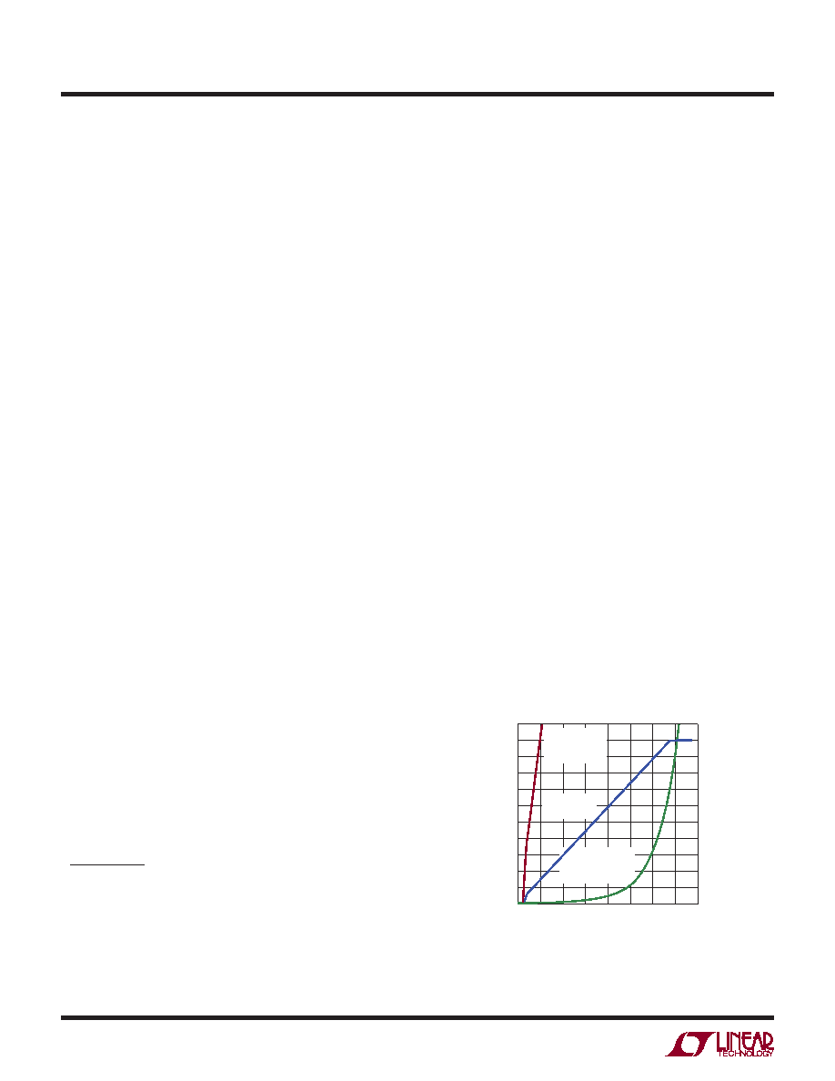
Ideal Diode from BAT to VOUT
The LTC4098-3.6 has an internal ideal diode as well as a
controller for an external ideal diode. Both the internal and
the external ideal diodes are always on and will respond
quickly whenever VOUT drops below BAT.
If the load current increases beyond the power allowed
from the switching regulator, additional power will be
pulled from the battery via the ideal diodes. Furthermore,
if power to VBUS (USB or wall power) is removed, then
all of the application power will be provided by the bat-
tery via the ideal diodes. The ideal diodes will be fast
enough to keep VOUT from drooping with only the stor-
age capacitance required for the switching regulator. The
internal ideal diode consists of a precision amplifier that
activates a large on-chip MOSFET transistor whenever
the voltage at VOUT is approximately 15mV (VFWD) below
the voltage at BAT. Within the amplifier’s linear range, the
small-signal resistance of the ideal diode will be quite low,
keeping the forward drop near 15mV. At higher current
levels, the MOSFET will be in full conduction. If additional
conductance is needed, an external P-channel MOSFET
FORWARD VOLTAGE (mV) (BAT – VOUT)
0
CURRENT
(mA)
600
1800
2000
2200
120
240 300
409836 F05
200
1400
1000
400
1600
0
1200
800
60
180
360
480
420
VISHAY Si2333
EXTERNAL
IDEAL DIODE
LTC4098-3.6
IDEAL DIODE
ON
SEMICONDUCTOR
MBRM120LT3
Figure 5. Ideal Diode V-I Characteristics
operaTion
相关PDF资料 |
PDF描述 |
|---|---|
| LTC4210-4IS6 | 1-CHANNEL POWER SUPPLY SUPPORT CKT, PDSO6 |
| LTC4210-3IS6 | 1-CHANNEL POWER SUPPLY SUPPORT CKT, PDSO6 |
| LTC4210-4CS6 | 1-CHANNEL POWER SUPPLY SUPPORT CKT, PDSO6 |
| LTC4355CMS#TRPBF | 2-CHANNEL POWER SUPPLY SUPPORT CKT, PDSO16 |
| LTC4355CMS#PBF | 2-CHANNEL POWER SUPPLY SUPPORT CKT, PDSO16 |
相关代理商/技术参数 |
参数描述 |
|---|---|
| LTC4099 | 制造商:LINER 制造商全称:Linear Technology 功能描述:I2C Controlled USB Power Manager/Charger with Overvoltage Protection |
| LTC4099EPDC#PBF | 功能描述:IC USB PWR MANAGER/CHRGR 20UTQFN RoHS:是 类别:集成电路 (IC) >> PMIC - 电池管理 系列:PowerPath™ 标准包装:1 系列:- 功能:充电管理 电池化学:锂离子(Li-Ion)、锂聚合物(Li-Pol) 电源电压:3.75 V ~ 6 V 工作温度:-40°C ~ 85°C 安装类型:表面贴装 封装/外壳:SC-74A,SOT-753 供应商设备封装:SOT-23-5 包装:剪切带 (CT) 产品目录页面:669 (CN2011-ZH PDF) 其它名称:MCP73831T-2ACI/OTCT |
| LTC4099EPDC#TRMPBF | 制造商:Linear Technology 功能描述: |
| LTC4099EPDC#TRPBF | 功能描述:IC USB PWR MANAGER/CHRGR 20UTQFN RoHS:是 类别:集成电路 (IC) >> PMIC - 电池管理 系列:PowerPath™ 标准包装:1 系列:- 功能:充电管理 电池化学:锂离子(Li-Ion)、锂聚合物(Li-Pol) 电源电压:3.75 V ~ 6 V 工作温度:-40°C ~ 85°C 安装类型:表面贴装 封装/外壳:SC-74A,SOT-753 供应商设备封装:SOT-23-5 包装:剪切带 (CT) 产品目录页面:669 (CN2011-ZH PDF) 其它名称:MCP73831T-2ACI/OTCT |
| LTC4099EPDC-PBF | 制造商:LINER 制造商全称:Linear Technology 功能描述:I2C Controlled USB Power Manager/Charger with Overvoltage Protection |
发布紧急采购,3分钟左右您将得到回复。