- 您现在的位置:买卖IC网 > PDF目录22137 > LTC4225IGN-1#TRPBF (Linear Technology)IC CTLR HOT SWAP DUAL 24-SSOP PDF资料下载
参数资料
| 型号: | LTC4225IGN-1#TRPBF |
| 厂商: | Linear Technology |
| 文件页数: | 14/24页 |
| 文件大小: | 346K |
| 描述: | IC CTLR HOT SWAP DUAL 24-SSOP |
| 标准包装: | 2,500 |
| 类型: | 热交换控制器 |
| 应用: | 通用 |
| 内部开关: | 无 |
| 电流限制: | 可调 |
| 电源电压: | 2.9 V ~ 18 V |
| 工作温度: | -40°C ~ 85°C |
| 安装类型: | 表面贴装 |
| 封装/外壳: | 24-SSOP(0.154",3.90mm 宽) |
| 供应商设备封装: | 24-SSOP |
| 包装: | 带卷 (TR) |
LTC4225-1/LTC4225-2
14
422512f
Supply Undervoltage Monitor
The ON pin functions as a turn-on control and an input
supply monitor. A resistive divider connected between
the input supply (IN1, IN2) and GND at the respective
ON pin monitors the supply undervoltage condition. The
undervoltage threshold is set by proper selection of the
resistors and is given by:
V
IN(UVTH)
= 1+
R
TOP
R
BOTTOM
?/DIV>
?/DIV>
?/DIV>
?/DIV>
?/DIV>
?/DIV>
V
ON(TH)
where V
ON(TH)
is the ON rising threshold (1.235V).
An undervoltage fault occurs if the input supply falls below
its undervoltage threshold for longer than 20祍. The FAULT
pin will not be pulled low. If the ON pin voltage falls below
1.155V but remains above 0.6V , the Hot Swap MOSFET is
turned off by a 300礎 pull-down from HGATE to ground.
The Hot Swap MOSFET turns back on instantly without
the 100ms debounce cycle when the input supply rises
above its undervoltage threshold.
However, if the ON pin voltage drops below 0.6V , it turns
off the Hot Swap MOSFET and clears the associated fault
latches. The Hot Swap MOSFET turns back on only after a
100ms debounce cycle when the input supply is restored
above its undervoltage threshold. An undervoltage fault on
one supply does not affect the operation of the other sup-
ply. The ideal diode function controlled by the ideal diode
MOSFET is unaffected by undervoltage fault conditions.
If both IN supplies fall until the internally generated sup-
ply, INTV
CC
, drops below its 2.2V UVLO threshold, all the
MOSFETs are turned off and the fault latches are cleared.
Operation resumes from a fresh start-up cycle when the
input supplies are restored and INTV
CC
exceeds its UVLO
threshold.
There is a 10祍 glitch filter on the ON pin to reject supply
glitches. By placing a filter capacitor, C
F
, with the resistive
divider at the ON pin, the glitch filter delay is further extended
by the RC time constant to prevent any false fault.
Power Good Monitor
Internal circuitry monitors the MOSFET gate overdrive
between the HGATE and OUT pins. The power good status
for each supply is reported via its respective open-drain
output, PWRGD1 or PWRGD2. They are normally pulled
high by an external pull-up resistor or the internal 10礎
pull-up. The power good output asserts low when the gate
overdrive exceeds 4.2V during the HGATE start-up. Once
asserted low, the power good status is latched and can only
be cleared by pulling the ON pin low, toggling the EN pin
from low to high, or INTV
CC
entering undervoltage lockout.
The power good output continues to pull low while HGATE
is regulating in active current limit, but pulls high when
the circuit breaker times out and pulls the HGATE pin low.
CPO and DGATE Start-Up
The CPO and DGATE pin voltages are initially pulled up to a
diode below the IN pin when first powered up. CPO starts
ramping up 7祍 after INTV
CC
clears its undervoltage lockout
level. Another 40祍 later, DGATE also starts ramping up
with CPO. The CPO ramp rate is determined by the CPO
pull-up current into the combined CPO and DGATE pin
capacitances. An internal clamp limits the CPO pin voltage
to 12V above the IN pin, while the final DGATE pin voltage
is determined by the gate drive amplifier. An internal 12V
clamp limits the DGATE pin voltage above IN.
applicaTions inForMaTion
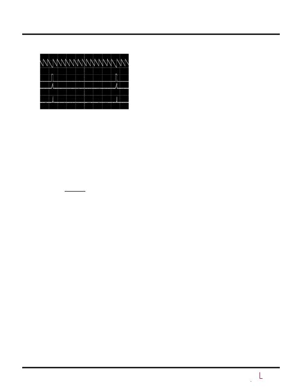
Figure 6. Auto-Retry Sequence After a Fault
TMR
1V/DIV
HGATE
5V/DIV
FAULT
10V/DIV
I
LOAD
20A/DIV
50ms/DIV
422512 F06
相关PDF资料 |
PDF描述 |
|---|---|
| VE-B2K-CY-B1 | CONVERTER MOD DC/DC 40V 50W |
| VE-23Y-CY-B1 | CONVERTER MOD DC/DC 3.3V 33W |
| GSM43DRTS | CONN EDGECARD 86POS DIP .156 SLD |
| VE-B2J-CY-B1 | CONVERTER MOD DC/DC 36V 50W |
| GMM43DRTS | CONN EDGECARD 86POS DIP .156 SLD |
相关代理商/技术参数 |
参数描述 |
|---|---|
| LTC4225IGN-2#PBF | 功能描述:IC CONTROLLER HOT SWAP 24-SSOP RoHS:是 类别:集成电路 (IC) >> PMIC - 热交换 系列:- 产品培训模块:Lead (SnPb) Finish for COTS Obsolescence Mitigation Program 标准包装:119 系列:- 类型:热交换控制器 应用:通用型,PCI Express? 内部开关:无 电流限制:- 电源电压:3.3V,12V 工作温度:-40°C ~ 85°C 安装类型:表面贴装 封装/外壳:80-TQFP 供应商设备封装:80-TQFP(12x12) 包装:托盘 产品目录页面:1423 (CN2011-ZH PDF) |
| LTC4225IGN-2#TRPBF | 功能描述:IC CTLR HOT SWAP DUAL 24-SSOP RoHS:是 类别:集成电路 (IC) >> PMIC - 热交换 系列:- 产品培训模块:Lead (SnPb) Finish for COTS Obsolescence Mitigation Program 标准包装:119 系列:- 类型:热交换控制器 应用:通用型,PCI Express? 内部开关:无 电流限制:- 电源电压:3.3V,12V 工作温度:-40°C ~ 85°C 安装类型:表面贴装 封装/外壳:80-TQFP 供应商设备封装:80-TQFP(12x12) 包装:托盘 产品目录页面:1423 (CN2011-ZH PDF) |
| LTC4225IUFD-1#PBF | 功能描述:IC CONTROLLER HOT SWAP 24-QFN RoHS:是 类别:集成电路 (IC) >> PMIC - 热交换 系列:- 标准包装:50 系列:- 类型:热交换控制器 应用:-48V 远程电力系统,AdvancedTCA ? 系统,高可用性 内部开关:无 电流限制:可调 电源电压:11.5 V ~ 14.5 V 工作温度:-40°C ~ 85°C 安装类型:表面贴装 封装/外壳:10-TFSOP,10-MSOP(0.118",3.00mm 宽) 供应商设备封装:10-MSOP 包装:管件 |
| LTC4225IUFD-1#TRPBF | 功能描述:IC CTLR HOT SWAP DUAL 24-QFN RoHS:是 类别:集成电路 (IC) >> PMIC - 热交换 系列:- 产品培训模块:Lead (SnPb) Finish for COTS Obsolescence Mitigation Program 标准包装:119 系列:- 类型:热交换控制器 应用:通用型,PCI Express? 内部开关:无 电流限制:- 电源电压:3.3V,12V 工作温度:-40°C ~ 85°C 安装类型:表面贴装 封装/外壳:80-TQFP 供应商设备封装:80-TQFP(12x12) 包装:托盘 产品目录页面:1423 (CN2011-ZH PDF) |
| LTC4225IUFD-2#PBF | 功能描述:IC CONTROLLER HOT SWAP 24-QFN RoHS:是 类别:集成电路 (IC) >> PMIC - 热交换 系列:- 产品培训模块:Lead (SnPb) Finish for COTS Obsolescence Mitigation Program 标准包装:119 系列:- 类型:热交换控制器 应用:通用型,PCI Express? 内部开关:无 电流限制:- 电源电压:3.3V,12V 工作温度:-40°C ~ 85°C 安装类型:表面贴装 封装/外壳:80-TQFP 供应商设备封装:80-TQFP(12x12) 包装:托盘 产品目录页面:1423 (CN2011-ZH PDF) |
发布紧急采购,3分钟左右您将得到回复。