- 您现在的位置:买卖IC网 > PDF目录19814 > LTC4232CDHC#PBF (Linear Technology)IC CTLR HOT SWAP 5A 16-DFN PDF资料下载
参数资料
| 型号: | LTC4232CDHC#PBF |
| 厂商: | Linear Technology |
| 文件页数: | 10/16页 |
| 文件大小: | 242K |
| 描述: | IC CTLR HOT SWAP 5A 16-DFN |
| 标准包装: | 73 |
| 类型: | 热交换开关 |
| 应用: | 服务器,储存,通信,嵌入式,消费品 |
| 内部开关: | 是 |
| 电流限制: | 可调 |
| 电源电压: | 2.9 V ~ 15 V |
| 工作温度: | 0°C ~ 70°C |
| 安装类型: | 表面贴装 |
| 封装/外壳: | 16-WFDFN 裸露焊盘 |
| 供应商设备封装: | 16-DFN(5x3) |
| 包装: | 管件 |
LTC4232
10
4232fa
applicaTions inForMaTion
An overcurrent fault occurs when the current limit circuitry
has been engaged for longer than the timeout delay set
by the TIMER. Current limiting begins when the MOSFET
current reaches 1.5A to 5.6A (depending on the foldback).
The GATE pin is then brought down with a 140mA GATE-
to-OUT current. The voltage on the GATE is regulated in
order to limit the current to less than 5.6A. At this point,
a circuit breaker time delay starts by charging the external
timing capacitor from the TIMER pin with a 100礎 pull-
up current. If the TIMER pin reaches its 1.2V threshold,
the internal switch turns off (with a 250礎 current from
GATE to ground). Included in the Typical Performance
Characteristics curves is a graph of the Safe Operating
Area for the MOSFET. From this graph one can determine
the MOSFETs maximum time in current limit for a given
output power.
Tying the TIMER pin to INTV
CC
will force the part to use
the internally generated (circuit breaker) delay of 2ms. In
either case the FLT pin is pulled low to indicate an over-
current fault has turned off the pass MOSFET. For a given
the circuit breaker time delay, the equation for setting the
timing capacitors value is as follows:
C
T
= t
CB
" 0.083(礔/ms)
After the switch is turned off, the TIMER pin begins
discharging the timing capacitor with a 2礎 pull-down
current. When the TIMER pin reaches its 0.2V threshold,
an internal 100ms timer is started. After the 100ms delay,
the switch is allowed to turn on again if the overcurrent
fault has been cleared. Bringing the UV pin below 0.6V
and then high will clear the fault. If the TIMER pin is tied
to INTV
CC
then the switch is allowed to turn on again (after
an internal 100ms delay) if the overcurrent fault is cleared.
Tying the FLT pin to the UV pin allows the part to self-
clear the fault and turn the MOSFET on as soon as TIMER
pin has ramped below 0.2V. In this auto-retry mode the
LTC4232 repeatedly tries to turn on after an overcurrent
at a period determined by the capacitor on the TIMER pin.
The auto-retry mode also functions when the TIMER pin
is tied to INTV
CC
.
The waveform in Figure 4 shows how the output latches
off following a short-circuit. The current in the MOSFET
is 1.4A as the timer ramps up.
10礔, especially if the wiring inductance from the supply
to the V
DD
pin is greater than 3礖. The possibility of oscil-
lation will increase as the load current (during power-up)
increases. There are two ways to prevent this type of
oscillation. The simplest way is to avoid load capacitances
below 10礔. For wiring inductance larger than 20礖, the
minimum load capacitance may extend to 100礔. A second
choice is to connect an external gate capacitor C
P
>1.5nF
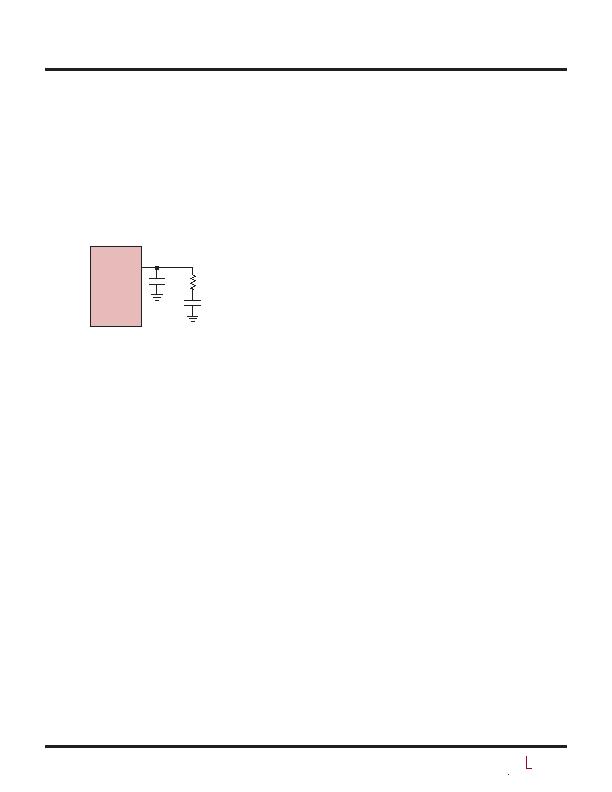
as shown in Figure 3.
Figure 3. Compensation for Small C
LOAD
4232 F03
LTC4232
*OPTIONAL
RC TO LOWER
INRUSH CURRENT
GATE
C
P
2.2nF
Turn-Off Sequence
The switch can be turned off by a variety of conditions. A
normal turn-off is initiated by the UV pin going below its
1.235V threshold. Additionally, several fault conditions
will turn off the switch. These include an input overvolt-
age (OV pin), overcurrent circuit breaker (SENSE pin) or
overtemperature. Normally the switch is turned off with
a 250礎 current pulling down the GATE pin to ground.
With the switch turned off, the OUT voltage drops which
pulls the FB pin below its threshold. PG then pulls low to
indicate output power is no longer good.
If V
DD
drops below 2.65V for greater than 5祍 or INTV
CC
drops below 2.5V for greater than 1祍, a fast shutdown
of the switch is initiated. The GATE is pulled down with a
140mA current to the OUT pin.
Overcurrent Fault
The LTC4232 features an adjustable current limit with
foldback that protects against short-circuits or excessive
load current. To prevent excessive power dissipation in the
switch during active current limit, the available current is
reduced as a function of the output voltage sensed by the
FB pin. A graph in the Typical Performance Characteristics
curves shows the current limit versus FB voltage.
相关PDF资料 |
PDF描述 |
|---|---|
| MAX6471TA25AD3+T | IC REG LDO 2.5V/ADJ .3A 8-TDFN |
| GMM43DSEI | CONN EDGECARD 86POS .156 EYELET |
| FSDM07652REWDTU | IC SWIT PWM GREEN CM HV TO220F |
| TAP335K016GSB | CAP TANT 3.3UF 16V 10% RADIAL |
| MAX6469TA33AD3+T | IC REG LDO 3.3V/ADJ .3A 8-TDFN |
相关代理商/技术参数 |
参数描述 |
|---|---|
| LTC4232IDHC#PBF | 功能描述:IC CTLR HOT SWAP 5A 16-DFN RoHS:是 类别:集成电路 (IC) >> PMIC - 热交换 系列:- 产品培训模块:Lead (SnPb) Finish for COTS Obsolescence Mitigation Program 标准包装:119 系列:- 类型:热交换控制器 应用:通用型,PCI Express? 内部开关:无 电流限制:- 电源电压:3.3V,12V 工作温度:-40°C ~ 85°C 安装类型:表面贴装 封装/外壳:80-TQFP 供应商设备封装:80-TQFP(12x12) 包装:托盘 产品目录页面:1423 (CN2011-ZH PDF) |
| LTC4232IDHC#TRPBF | 功能描述:IC CTLR HOT SWAP 5A 16-DFN RoHS:是 类别:集成电路 (IC) >> PMIC - 热交换 系列:- 产品培训模块:Lead (SnPb) Finish for COTS Obsolescence Mitigation Program 标准包装:119 系列:- 类型:热交换控制器 应用:通用型,PCI Express? 内部开关:无 电流限制:- 电源电压:3.3V,12V 工作温度:-40°C ~ 85°C 安装类型:表面贴装 封装/外壳:80-TQFP 供应商设备封装:80-TQFP(12x12) 包装:托盘 产品目录页面:1423 (CN2011-ZH PDF) |
| LTC4240 | 制造商:LINER 制造商全称:Linear Technology 功能描述:CompactPCI Hot Swap Controller with I2C Compatible Interface |
| LTC4240CGN | 功能描述:IC CTRLR HOTSWAP CPCI I2C 28SSOP RoHS:否 类别:集成电路 (IC) >> PMIC - 热交换 系列:- 产品培训模块:Lead (SnPb) Finish for COTS Obsolescence Mitigation Program 标准包装:119 系列:- 类型:热交换控制器 应用:通用型,PCI Express? 内部开关:无 电流限制:- 电源电压:3.3V,12V 工作温度:-40°C ~ 85°C 安装类型:表面贴装 封装/外壳:80-TQFP 供应商设备封装:80-TQFP(12x12) 包装:托盘 产品目录页面:1423 (CN2011-ZH PDF) |
| LTC4240CGN#PBF | 功能描述:IC CTLR HOT SWAP CPCI I2C 28SSOP RoHS:是 类别:集成电路 (IC) >> PMIC - 热交换 系列:- 产品培训模块:Lead (SnPb) Finish for COTS Obsolescence Mitigation Program 标准包装:119 系列:- 类型:热交换控制器 应用:通用型,PCI Express? 内部开关:无 电流限制:- 电源电压:3.3V,12V 工作温度:-40°C ~ 85°C 安装类型:表面贴装 封装/外壳:80-TQFP 供应商设备封装:80-TQFP(12x12) 包装:托盘 产品目录页面:1423 (CN2011-ZH PDF) |
发布紧急采购,3分钟左右您将得到回复。