- 您现在的位置:买卖IC网 > PDF目录19738 > LTC4241IGN#TRPBF (Linear Technology)IC CTRLR HOTSWAP 3.3V AUX 20SSOP PDF资料下载
参数资料
| 型号: | LTC4241IGN#TRPBF |
| 厂商: | Linear Technology |
| 文件页数: | 11/16页 |
| 文件大小: | 279K |
| 描述: | IC CTRLR HOTSWAP 3.3V AUX 20SSOP |
| 标准包装: | 2,500 |
| 类型: | 热交换控制器 |
| 应用: | PCI,PCI-X |
| 内部开关: | 无 |
| 电源电压: | 3.3V,5V,±12V |
| 工作温度: | -40°C ~ 85°C |
| 安装类型: | 表面贴装 |
| 封装/外壳: | 20-SSOP(0.154",3.90mm 宽) |
| 供应商设备封装: | 20-SSOP |
| 包装: | 带卷 (TR) |
LTC4241
11
sn4241 4241f
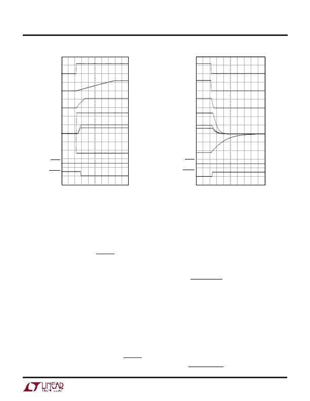
Timer
During a power-up sequence for the PCI power supplies,
a 22礎 current source is connected to the TIMER pin and
current limit faults are ignored until the voltage ramps to
within 0.9V of 12V
IN
. This feature allows the chip to power
up a PCI slot that can accommodate boards with a wide
range of capacitive loads on the supplies. The power-up
time for any one of the four outputs will be:
C
V
I
I
ON
LOAD OUT
LIMIT LOAD
E
?/DIV>
?/DIV>
?/DIV>
?/DIV>
?/DIV>
?/DIV>
2"
"
For example, for C
LOAD
= 2000礔, V
OUT
= 5V, I
LIMIT
= 7A,
I
LOAD
= 5A, the 5V
OUT
turn-on time will be ~10ms. By
substituting the variables in the above equation with the
appropriate values, the turn-on time for the other three
outputs can be calculated. The timer period should be set
longer than the maximum supply turn-on time but short
enough to not exceed the maximum safe operating area of
the pass transistor during a short-circuit. The timer period
is given by:
APPLICATIO S I FOR ATIO
U
U
U
The current in each pass transistor increases until it
reaches the current limit for each supply. Each supply is
allowed to power up at the rate dV/dt = 60礎/C1 or as
determined by the current limit and the load capacitance
on the supply line, whichever is slower. Current limit faults
are ignored while the TIMER pin voltage is ramping up and
is less than 0.9V below 12V
IN
. Once all four PCI supply
voltages are within tolerance, the PWRGD pin will pull low.
Power-Down Sequence for PCI Power Supplies
When the ON pin is pulled low, a power-down sequence
begins for all the PCI power supplies (Figure 3).
Internal switches are connected to each of the output
supply voltage pins to discharge the load capacitors to
ground. The TIMER pin is immediately pulled low and the
internal 12V and 12V switches are turned off. The GATE
pin is pulled to ground by an internal 200礎 current
source. This turns off the external pass transistors in a
controlled manner and prevents the load current on the
3.3V and 5V supplies from going to zero instantaneously
and glitching the power supply voltages. When any of the
output voltages dips below its threshold, the PWRGD pin
pulls high.
Figure 2. Normal Power-Up Sequence
Figure 3. Normal Power-Down Sequence
ON
10V/DIV
TIMER
10V/DIV
GATE
10V/DIV
PWRGD
10V/DIV
5V
OUT
5V/DIV
3V
OUT
5V/DIV
12V
OUT
5V/DIV
V
EEOUT
5V/DIV
FAULT
10V/DIV
10ms/DIV
4241 F03
t
C
V
A
TIMER
TIMER
=
?/DIV>
" .
11 1
22
ON
10V/DIV
TIMER
10V/DIV
GATE
10V/DIV
PWRGD
10V/DIV
5V
OUT
5V/DIV
3V
OUT
5V/DIV
12V
OUT
5V/DIV
V
EEOUT
5V/DIV
FAULT
10V/DIV
10ms/DIV
4241 F02
相关PDF资料 |
PDF描述 |
|---|---|
| MIC2954-02BZ TR | IC REG LDO 5V .25A TO92-3 |
| MIC2954-02BT | IC REG LDO 5V .25A TO220-3 |
| CDRH104RNP-470NC | INDUCTOR POWER 47UH 2.10A SMD |
| MIC2954-02BS TR | IC REG LDO 5V .25A SOT-223 |
| TNY266GN | IC OFFLINE SWIT OTP OCP HV 8SMD |
相关代理商/技术参数 |
参数描述 |
|---|---|
| LTC4242 | 制造商:LINER 制造商全称:Linear Technology 功能描述:Dual Slot Hot Swap Controller for PCI Express |
| LTC4242CG | 制造商:LINER 制造商全称:Linear Technology 功能描述:Dual Slot Hot Swap Controller for PCI Express |
| LTC4242CG#PBF | 功能描述:IC CNTRLR HOT SWAP 36-SSOP RoHS:是 类别:集成电路 (IC) >> PMIC - 热交换 系列:- 产品培训模块:Obsolescence Mitigation Program 标准包装:100 系列:- 类型:热插拔开关 应用:通用 内部开关:是 电流限制:可调 电源电压:9 V ~ 13.2 V 工作温度:-40°C ~ 150°C 安装类型:表面贴装 封装/外壳:10-WFDFN 裸露焊盘 供应商设备封装:10-TDFN-EP(3x3) 包装:管件 |
| LTC4242CG#TRPBF | 功能描述:IC CNTRLR HOT SWAP 36-SSOP RoHS:是 类别:集成电路 (IC) >> PMIC - 热交换 系列:- 产品培训模块:Obsolescence Mitigation Program 标准包装:100 系列:- 类型:热插拔开关 应用:通用 内部开关:是 电流限制:可调 电源电压:9 V ~ 13.2 V 工作温度:-40°C ~ 150°C 安装类型:表面贴装 封装/外壳:10-WFDFN 裸露焊盘 供应商设备封装:10-TDFN-EP(3x3) 包装:管件 |
| LTC4242CUHF | 制造商:LINER 制造商全称:Linear Technology 功能描述:Dual Slot Hot Swap Controller for PCI Express |
发布紧急采购,3分钟左右您将得到回复。