- 您现在的位置:买卖IC网 > PDF目录19849 > LTC4268IDKD-1#TRPBF (Linear Technology)IC PD HIGH POWER W/CNTRL 32-DFN PDF资料下载
参数资料
| 型号: | LTC4268IDKD-1#TRPBF |
| 厂商: | Linear Technology |
| 文件页数: | 42/46页 |
| 文件大小: | 419K |
| 描述: | IC PD HIGH POWER W/CNTRL 32-DFN |
| 标准包装: | 2,500 |
| 类型: | 以太网供电开关(PoE) |
| 应用: | 远程外设(工业控制,相机,数据访问) |
| 内部开关: | 是 |
| 工作温度: | -40°C ~ 85°C |
| 安装类型: | 表面贴装 |
| 封装/外壳: | 32-WFDFN 裸露焊盘 |
| 供应商设备封装: | 32-DFN(7x4)裸露焊盘 |
| 包装: | 带卷 (TR) |
第1页第2页第3页第4页第5页第6页第7页第8页第9页第10页第11页第12页第13页第14页第15页第16页第17页第18页第19页第20页第21页第22页第23页第24页第25页第26页第27页第28页第29页第30页第31页第32页第33页第34页第35页第36页第37页第38页第39页第40页第41页当前第42页第43页第44页第45页第46页
LTC4268-1
42
42681fc
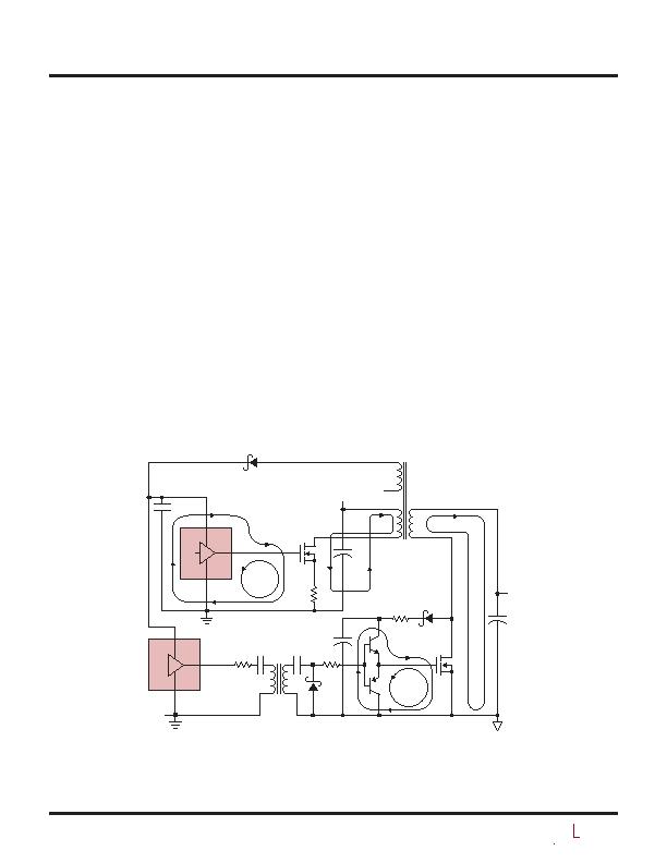
In order to minimize switching noise and improve output
load regulation, connect the GND pin of the LTC4268-1
directly to the ground terminal of the V
CC
decoupling
capacitor, the bottom terminal of the current sense resistor
and the ground terminal of the input capacitor, using a
ground plane with multiple vias. Place the V
CC
capacitor
immediately adjacent to the V
CC
and GND pins on the IC
package. This capacitor carries high di/dt MOSFET gate
drive currents. Use a low ESR ceramic capacitor. Take care
in PCB layout to keep the traces that conduct high switching
currents short, wide and with minimal overall loop area.
These are typically the traces associated with the switches.
This reduces the parasitic inductance and also minimizes
magnetic field radiation. Figure 21 outlines the critical paths.
Keep electric field radiation low by minimizing the length
and area of traces (keep stray capacitances low). The drain
of the primary side MOSFET is the worst offender in this
category. Always use a ground plane under the switcher
circuitry to prevent coupling between PCB planes. Check
that the maximum BV
DSS
ratings of the MOSFETs are not
exceeded due to inductive ringing. This is done by viewing
the MOSFET node voltages with an oscilloscope. If it is
breaking down either choose a higher voltage device, add
a snubber or specify an avalanche-rated MOSFET.
Place the small-signal components away from high
frequency switching nodes. This allows the use of a pseudo-
Kelvin connection for the signal ground, where high di/
dt gate driver currents flow out of the IC ground pin in
one direction (to the bottom plate of the V
CC
decoupling
capacitor) and small-signal currents flow in the other
direction. Keep the trace from the feedback divider tap
to the FB pin short to preclude inadvertent pickup. For
applications with multiple switching power converters
connected to the same input supply, make sure that the
input filter capacitor for the LTC4268-1 is not shared with
other converters. AC input current from another converter
could cause substantial input voltage ripple and this could
interfere with the LTC4268-1 operation. A few inches of PC
trace or wire (L @100nH) between the C
IN
of the LTC4268-1
and the actual source V
IN
is sufficient to prevent current
sharing problems.
T2
T1
C
R
C
VIN
MS
MP
GATE
TURN-ON
GATE
TURN-ON
R
SENSE
" "
C
VCC
SG
V
CC
PG
V
CC
V
CC
V
CC
V
IN
GATE
TURN-OFF
GATE
TURN-OFF
Q4
Q3
C
OUT
42681 F21
OUT
"
"
"
+
+
+
Figure 21. Layout Critical High Current Paths
applicaTions inForMaTion
相关PDF资料 |
PDF描述 |
|---|---|
| S102M25Z5UN6TJ6R | CAP CER 1000PF 1KV 20% RADIAL |
| MAX8860EUA18+T | IC REG LDO 1.8V/ADJ .3A 8-UMAX |
| VI-J13-CW-B1 | CONVERTER MOD DC/DC 24V 100W |
| F152K43Y5RN6TJ7R | CAP CER 1500PF 1KV 10% RADIAL |
| RSM31DTAI-S189 | CONN EDGECARD 62POS R/A .156 SLD |
相关代理商/技术参数 |
参数描述 |
|---|---|
| LTC4269-1 | 制造商:LINER 制造商全称:Linear Technology 功能描述:IEEE 802.3at PD with Synchronous No-Opto Flyback Controller |
| LTC4269-2 | 制造商:LINER 制造商全称:Linear Technology 功能描述:IEEE 802.3at High Power PD and Synchronous Forward Controller with AUX Support |
| LTC4269CDKD-1#PBF | 功能描述:IC PD/OPTO FLYBACK CTRLR 32-DFN RoHS:是 类别:集成电路 (IC) >> PMIC - 热交换 系列:- 标准包装:50 系列:- 类型:热交换控制器 应用:-48V 远程电力系统,AdvancedTCA ? 系统,高可用性 内部开关:无 电流限制:可调 电源电压:11.5 V ~ 14.5 V 工作温度:-40°C ~ 85°C 安装类型:表面贴装 封装/外壳:10-TFSOP,10-MSOP(0.118",3.00mm 宽) 供应商设备封装:10-MSOP 包装:管件 |
| LTC4269CDKD-1#TRPBF | 功能描述:IC PD/OPTO FLYBACK CTRLR 32-DFN RoHS:是 类别:集成电路 (IC) >> PMIC - 热交换 系列:- 产品培训模块:Obsolescence Mitigation Program 标准包装:100 系列:- 类型:热插拔开关 应用:通用 内部开关:是 电流限制:可调 电源电压:9 V ~ 13.2 V 工作温度:-40°C ~ 150°C 安装类型:表面贴装 封装/外壳:10-WFDFN 裸露焊盘 供应商设备封装:10-TDFN-EP(3x3) 包装:管件 |
| LTC4269CDKD-1-PBF | 制造商:LINER 制造商全称:Linear Technology 功能描述:IEEE 802.3at PD with Synchronous No-Opto Flyback Controller |
发布紧急采购,3分钟左右您将得到回复。