参数资料
| 型号: | LTC4312IMS#TRPBF |
| 厂商: | Linear Technology |
| 文件页数: | 2/20页 |
| 文件大小: | 0K |
| 描述: | IC MULTIPLEXER 16-MSOP |
| 标准包装: | 2,500 |
| 系列: | * |
LTC4312
10
4312f
APPLICATIONS INFORMATION
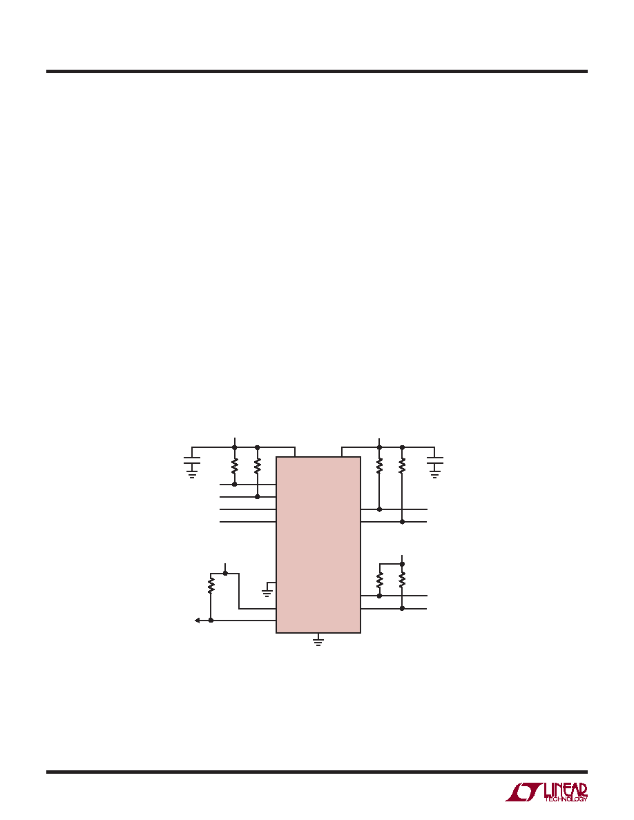
Figure 3. Connection of the LTC4312 in a Level Shift Application. VCC2 Is
Less Than or Equal to the Minimum Bus Supply Voltage on the Output Side
If VCC2 is tied low, the output side rise time accelerators
are disabled independent of the state of the ACC pin.
ACC tied high disables input and output RTAs. Using a
combination of the ACC pin and the VCC2 voltage allows
the user independent control of the input and output side
rise time accelerators. The rise time accelerators are also
internally disabled during power-up and VCC2 transitions,
as described in the Operation section, as well as during
automatic clocking and stop bit generation for a bus stuck
low recovery event.
The rise time accelerators when activated pull the bus up
to 0.9VCC on the input side of the SDA and SCL lines.
On the output side the SDAOUT and SCLOUT lines are
pulled up by the rise time accelerators to 0.8VCC2. For
VCC2 voltages approaching 2.3V, acceleration of the output
bus may not be seen all the way to 0.8VCC2 due to the
threshold voltage of the NFET pass device.
Supply Voltage Considerations in Level Translation
Applications
Care must be taken to ensure that the bus supply voltages
on the input and output sides are greater than 0.9VCC and
0.8VCC2, respectively, to ensure that the bus is not driven
above the bus supplies by the rise time accelerators. This
is usually accomplished in a level shifting application by
tying VCC to the input bus supply and VCC2 to the minimum
bus supply on the output side as shown in Figure 3.
If VCC2isgrounded,themultiplexerpassgatesarepowered
from VCC. In this case the minimum output bus supply
of the enabled channels should be greater than or equal
to VCC to prevent cross-conduction between the enabled
output channels. This is shown in Figure 4. Grounding VCC2
as shown in Figure 4 disables the output side rise time
accelerators independent of the state of the ACC pin. The
input rise time accelerators in this conguration continue
to be controlled by the ACC pin and can be enabled inde-
pendently. In Figure 4, ACC is left open to obtain a high VIL
and a 3mA rise time accelerator current on the input side.
LTC4312
GND
VCC
VCC2
4312 F03
SCLOUT1
SDAOUT1
SCLOUT2
SDAOUT2
SCLOUT1
SDAOUT1
SCLOUT2
SDAOUT2
SCLIN
SDAIN
ENABLE1
ENABLE2
ACC
DISCEN
FAULT
SCLIN
SDAIN
ENABLE1
ENABLE2
3.3V
FAULT
R3
10k
R2
10k
R1
10k
C1
0.01μF
3.3V
R5
10k
R4
10k
C2
0.01μF
5V
R7
10k
R6
10k
相关PDF资料 |
PDF描述 |
|---|---|
| LTC4313IMS8-1#PBF | IC 2WIRE BUS BUFFER 8MSOP |
| LTC4314IGN#PBF | IC MULTIPLEXER 20-MSOP |
| LTC4315IMS#TRPBF | IC 2WIRE BUS BUFFER 12MSOP |
| LTC485IS8#TRPBF | IC TXRX INTRFC RS485 LOPWR 8SOIC |
| LTC487IN#PBF | IC DVR RS485 LOW PWR QUAD 16-DIP |
相关代理商/技术参数 |
参数描述 |
|---|---|
| LTC4313CDD-1#PBF | 功能描述:IC 2WIRE BUS BUFFER 8DFN RoHS:是 类别:集成电路 (IC) >> 接口 - 信号缓冲器,中继器,分配器 系列:- 标准包装:160 系列:- 类型:转发器 Tx/Rx类型:以太网 延迟时间:- 电容 - 输入:- 电源电压:2.37 V ~ 2.63 V 电流 - 电源:60mA 安装类型:表面贴装 封装/外壳:64-TQFP 裸露焊盘 供应商设备封装:64-TQFP-EP(10x10) 包装:托盘 其它名称:Q5134101 |
| LTC4313CDD-1#TRPBF | 功能描述:IC 2WIRE BUS BUFFER 8DFN RoHS:是 类别:集成电路 (IC) >> 接口 - 信号缓冲器,中继器,分配器 系列:- 标准包装:160 系列:- 类型:转发器 Tx/Rx类型:以太网 延迟时间:- 电容 - 输入:- 电源电压:2.37 V ~ 2.63 V 电流 - 电源:60mA 安装类型:表面贴装 封装/外壳:64-TQFP 裸露焊盘 供应商设备封装:64-TQFP-EP(10x10) 包装:托盘 其它名称:Q5134101 |
| LTC4313CDD-2#PBF | 功能描述:IC 2WIRE BUS BUFFER 8DFN RoHS:是 类别:集成电路 (IC) >> 接口 - 信号缓冲器,中继器,分配器 系列:- 标准包装:160 系列:- 类型:转发器 Tx/Rx类型:以太网 延迟时间:- 电容 - 输入:- 电源电压:2.37 V ~ 2.63 V 电流 - 电源:60mA 安装类型:表面贴装 封装/外壳:64-TQFP 裸露焊盘 供应商设备封装:64-TQFP-EP(10x10) 包装:托盘 其它名称:Q5134101 |
| LTC4313CDD-2#TRPBF | 功能描述:IC 2WIRE BUS BUFFER 8DFN RoHS:是 类别:集成电路 (IC) >> 接口 - 信号缓冲器,中继器,分配器 系列:- 标准包装:160 系列:- 类型:转发器 Tx/Rx类型:以太网 延迟时间:- 电容 - 输入:- 电源电压:2.37 V ~ 2.63 V 电流 - 电源:60mA 安装类型:表面贴装 封装/外壳:64-TQFP 裸露焊盘 供应商设备封装:64-TQFP-EP(10x10) 包装:托盘 其它名称:Q5134101 |
| LTC4313CDD-3#PBF | 功能描述:IC 2WIRE BUS BUFFER 8DFN RoHS:是 类别:集成电路 (IC) >> 接口 - 信号缓冲器,中继器,分配器 系列:- 标准包装:160 系列:- 类型:转发器 Tx/Rx类型:以太网 延迟时间:- 电容 - 输入:- 电源电压:2.37 V ~ 2.63 V 电流 - 电源:60mA 安装类型:表面贴装 封装/外壳:64-TQFP 裸露焊盘 供应商设备封装:64-TQFP-EP(10x10) 包装:托盘 其它名称:Q5134101 |
发布紧急采购,3分钟左右您将得到回复。