参数资料
| 型号: | LTC6088CGN#TRPBF |
| 厂商: | Linear Technology |
| 文件页数: | 16/16页 |
| 文件大小: | 0K |
| 描述: | IC AMP QUAD CMOS R-R 16-SSOP |
| 标准包装: | 2,500 |
| 放大器类型: | 通用 |
| 电路数: | 4 |
| 输出类型: | 满摆幅 |
| 转换速率: | 7.2 V/µs |
| 增益带宽积: | 14MHz |
| 电流 - 输入偏压: | 1pA |
| 电压 - 输入偏移: | 330µV |
| 电流 - 电源: | 1.05mA |
| 电流 - 输出 / 通道: | 45mA |
| 电压 - 电源,单路/双路(±): | 2.7 V ~ 5.5 V |
| 工作温度: | 0°C ~ 70°C |
| 安装类型: | 表面贴装 |
| 封装/外壳: | 16-SSOP(0.154",3.90mm 宽) |
| 供应商设备封装: | 16-SSOP |
| 包装: | 带卷 (TR) |
LTC6087/LTC6088
9
60878fc
pin Functions
OUT: Amplifier Output.
–IN: Inverting Input.
+IN: Noninverting Input.
V+: Positive Supply.
V–: Negative Supply.
SHDNA: Shutdown Pin of Amplifier A, active low and only
available with the LTC 6087DD. An internal current source
pulls the pin to V+ when floating.
SHDNB: Shutdown Pin of Amplifier B, active low and only
available with the LTC 6087DD. An internal current source
pulls the pin to V+ when floating.
NC: Not internally connected
Exposed Pad: Connected to V–.
Rail-to-Rail Input
TheinputstageofLTC6087/LTC6088combinesbothPMOS
and NMOS differential pairs, extending its input common
modevoltagetobothpositiveandnegativesupplyvoltages.
At high input common mode range, the NMOS pair is on.
At low common mode range, the PMOS pair is on. The
transition happens when the common voltage is between
1.3V and 0.9V below the positive supply.
Achieving Low Input Bias Current
The DD and DHC packages are leadless and make contact
to the PCB beneath the package. Solder flux used during
the attachment of the part to the PCB can create leakage
current paths and can degrade the input bias current per-
formance of the part. All inputs are susceptible because
the backside paddle is connected to V– internally. As the
input voltage or V– changes, a leakage path can be formed
and alter the observed input bias current. For lowest bias
current use the LTC6087/LTC6088 in the leaded MSOP/
GN package. With fine PCB design rules, you can also
provide a guard ring around the inputs.
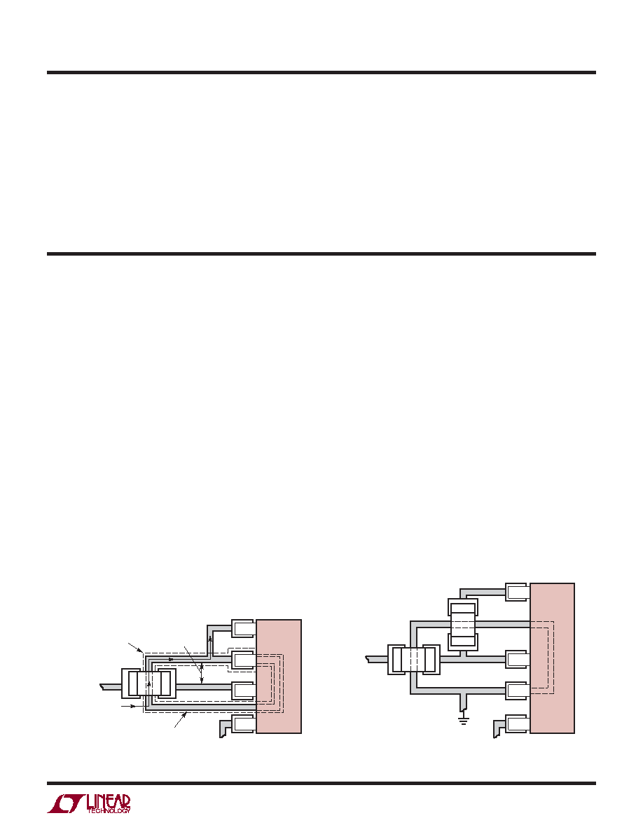
For example, in high source impedance applications such
as pH probes, photo diodes, strain gauges, et cetera, the
low input bias current of these parts requires a clean
board layout to minimize additional leakage current into a
high impedance signal node. A mere 100G
Ω of PC board
resistance between a 5V supply trace and input trace near
ground potential adds 50pA of leakage current. This leak-
age is far greater than the bias current of the operational
amplifier. A guard ring around the high impedance input
traces driven by a low impedance source equal to the
input voltage prevents such leakage problems. The guard
ring should extend as far as necessary to shield the high
impedance signal from any and all leakage paths. Figure
1 shows the use of a guard ring in a unity-gain configura-
tion. In this case the guard ring is connected to the output
and is shielding the high impedance noninverting input
from V–. Figure 2 shows the inverting gain configuration.
Figure 1. Sample Layout. Unity-Gain Configuration. Using Guard
Ring to Shield High Impedance Input from Board Leakage
Figure 2. Sample Layout. Inverting Gain Configuration. Using
Guard Ring to Shield High Impedance Input from Board Leakage
applications inForMation
LTC6087
R
OUT
IN–
IN+
V–
LEAKAGE
CURRENT
NO LEAKAGE
CURRENT
GUARD
RING
NO SOLDER MASK
OVER THE GUARD RING
60878 F01
LTC6087
60878 F02
R
OUT
IN–
IN+
V–
VIN
GND
相关PDF资料 |
PDF描述 |
|---|---|
| FHP-23-02-T-S | CONN RCPT .156" 23POS TIN SMD |
| LTC6240CS8#PBF | IC OP AMP SNGL R-R 8-SOIC |
| SMS05T1G | TVS ARRAY QUAD 350W SC74-6 |
| FBA09A12H1A | FAN 12VDC 2.7W 92MM FBA HYDRO |
| 302-R641 | CONN HEADER R/A 64POS GOLD |
相关代理商/技术参数 |
参数描述 |
|---|---|
| LTC6088HDHC#PBF | 功能描述:IC AMP CMOS QUAD R-R 16-DFN RoHS:是 类别:集成电路 (IC) >> Linear - Amplifiers - Instrumentation 系列:- 产品培训模块:Differential Circuit Design Techniques for Communication Applications 标准包装:1 系列:- 放大器类型:RF/IF 差分 电路数:1 输出类型:差分 转换速率:9800 V/µs 增益带宽积:- -3db带宽:2.9GHz 电流 - 输入偏压:3µA 电压 - 输入偏移:- 电流 - 电源:40mA 电流 - 输出 / 通道:- 电压 - 电源,单路/双路(±):3 V ~ 3.6 V 工作温度:-40°C ~ 85°C 安装类型:表面贴装 封装/外壳:16-VQFN 裸露焊盘,CSP 供应商设备封装:16-LFCSP-VQ 包装:剪切带 (CT) 产品目录页面:551 (CN2011-ZH PDF) 其它名称:ADL5561ACPZ-R7CT |
| LTC6088HDHC#TRPBF | 功能描述:IC AMP QUAD CMOS R-R 16-DFN RoHS:是 类别:集成电路 (IC) >> Linear - Amplifiers - Instrumentation 系列:- 标准包装:1 系列:- 放大器类型:通用 电路数:4 输出类型:满摆幅 转换速率:0.6 V/µs 增益带宽积:1MHz -3db带宽:- 电流 - 输入偏压:2pA 电压 - 输入偏移:1000µV 电流 - 电源:85µA 电流 - 输出 / 通道:20mA 电压 - 电源,单路/双路(±):1.8 V ~ 6 V 工作温度:-40°C ~ 125°C 安装类型:表面贴装 封装/外壳:14-SOIC(0.154",3.90mm 宽) 供应商设备封装:14-SOICN 包装:剪切带 (CT) 产品目录页面:680 (CN2011-ZH PDF) 其它名称:MCP6L04T-E/SLCT |
| LTC6088HDHC-PBF | 制造商:LINER 制造商全称:Linear Technology 功能描述:Dual/Quad 14MHz, Rail-to-Rail CMOS Amplifi ers |
| LTC6088HDHC-TRPBF | 制造商:LINER 制造商全称:Linear Technology 功能描述:Dual/Quad 14MHz, Rail-to-Rail CMOS Amplifi ers |
| LTC6088HGN#PBF | 功能描述:IC AMP CMOS QUAD R-R 16-SSOP RoHS:是 类别:集成电路 (IC) >> Linear - Amplifiers - Instrumentation 系列:- 标准包装:50 系列:- 放大器类型:通用 电路数:2 输出类型:满摆幅 转换速率:1.8 V/µs 增益带宽积:6.5MHz -3db带宽:4.5MHz 电流 - 输入偏压:5nA 电压 - 输入偏移:100µV 电流 - 电源:65µA 电流 - 输出 / 通道:35mA 电压 - 电源,单路/双路(±):1.8 V ~ 5.25 V,±0.9 V ~ 2.625 V 工作温度:-40°C ~ 85°C 安装类型:表面贴装 封装/外壳:10-TFSOP,10-MSOP(0.118",3.00mm 宽) 供应商设备封装:10-MSOP 包装:管件 |
发布紧急采购,3分钟左右您将得到回复。