- 您现在的位置:买卖IC网 > PDF目录79749 > LTC6104CMS8 (LINEAR TECHNOLOGY CORP) 2-CHANNEL POWER SUPPLY SUPPORT CKT, PDSO8 PDF资料下载
参数资料
| 型号: | LTC6104CMS8 |
| 厂商: | LINEAR TECHNOLOGY CORP |
| 元件分类: | 电源管理 |
| 英文描述: | 2-CHANNEL POWER SUPPLY SUPPORT CKT, PDSO8 |
| 封装: | PLASTIC, MSOP-8 |
| 文件页数: | 16/16页 |
| 文件大小: | 304K |
| 代理商: | LTC6104CMS8 |

LTC6104
9
6104f
APPLICATIONS INFORMATION
Selection of External Input Resistor, RIN
The external input resistor, RIN, controls the trans-
conductance of the current sense circuit.
Since I
transconductance g
OUT
m
==
V
R
SENSE
IN
,
1
R
For example if R
then I
V
IN
OUT
S
,,
==
100
E
ENSE
OUT
SENSE
or
I
mA for V
mV
100
1
100
.
=±
RIN should be chosen to allow the required resolution
while limiting the output current. At low supply voltage,
IOUT may be as much as ±1mA. By setting RIN such that
the largest expected sense voltage gives IOUT = ±1mA,
then the maximum output dynamic range is available.
Output dynamic range is limited by both the maximum
allowed output current and the maximum allowed output
voltage, as well as the minimum practical output signal. If
less dynamic range is required, then RIN can be increased
accordingly, reducing the maximum output current and
power dissipation. If low sense currents must be resolved
accurately in a system that has very wide dynamic range,
a smaller RIN than the maximum current specication
allows may be used if the maximum current is limited in
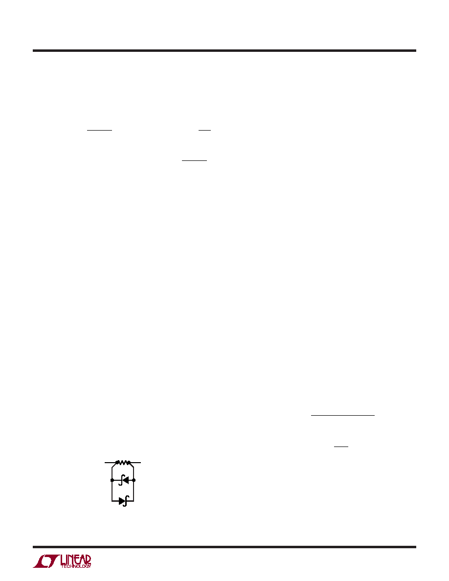
another way, such as with a Schottky diode across RSENSE
(Figure 3). This will reduce the high current measurement
accuracy by limiting the result, while increasing the low
current measurement resolution. This approach can be
helpful in cases where occasional large burst currents
may be ignored.
Care should be taken when designing the printed circuit
board layout to minimize input trace resistance (to Pins
5, 6, 7 and 8). Trace and interconnect impedances to the
–IN terminals will increase the effective RIN value, causing
a gain error, especially for small RIN values. In addition,
internal device resistance will add approximately 0.3
Ω
to RIN.
Trace and interconnect impedances to the +INB terminal will
have an effect on offset error. These errors are described
in more detail later in this data sheet.
Selection of External Output Resistor, ROUT
The output resistor, ROUT, determines how the output cur-
rent is converted to voltage. VOUT is simply IOUT ROUT +
VREF. In choosing an output resistor, the maximum output
voltage range must rst be considered. If the circuit that
is driven by the output does not limit the output voltage
range, then ROUT must be chosen such that the maximum
output voltage range does not exceed the LTC6104 maxi-
mum output voltage range (see Electrical Characteristics).
If the following circuit is a buffer or ADC with limited input
range, then ROUT must be chosen so that VOUT is in the
allowed maximum input range of this circuit.
In addition, the output impedance is determined by ROUT.
If the circuit to be driven has high enough input imped-
ance, then almost any useful output impedance will be
acceptable. However, if the driven circuit has relatively low
input impedance, or draws spikes of current, such as an
ADC might do, then a lower ROUT value may be required
in order to preserve the accuracy of the output. As an
example, if the input impedance of the driven circuit is
100 times ROUT, then the accuracy of VOUT will be reduced
by 1% since:
VV
I
RR
OUT
REF
OUT
IN DRIVEN
OUT
IN DRI
–
()
(
=
+
V
VEN
OUT
IR
)
.
==
100
101
099
Selection of External Voltage Reference, VREF
Selection of external reference voltage should be consid-
ered together with selection of ROUT.
Example:
Given the conditions: IOUT = –1mA to 1mA, VS = 12V.
Figure 3. Shunt Diodes Limit Maximum Input Voltage to Allow
Better Low Input Resolution Without Overranging
DSENSE
RSENSE
BATTERY
6104 F03
LOAD
相关PDF资料 |
PDF描述 |
|---|---|
| LSN-0.8/15-D12H | 1-OUTPUT 12 W DC-DC REG PWR SUPPLY MODULE |
| LP3907SQX-JIXI | 1.5 A DUAL SWITCHING CONTROLLER, 2100 kHz SWITCHING FREQ-MAX, QCC24 |
| LT1004IPWRG4-1-2 | 1-OUTPUT TWO TERM VOLTAGE REFERENCE, 1.235 V, PDSO8 |
| LTC2912HDDB-3#PBF | 1-CHANNEL POWER SUPPLY SUPPORT CKT, PDSO8 |
| LK1501-9EPDD | 1-OUTPUT 150 W AC-DC REG PWR SUPPLY MODULE |
相关代理商/技术参数 |
参数描述 |
|---|---|
| LTC6104CMS8#PBF | 功能描述:IC AMP CURRENT SENSE 8-MSOP RoHS:是 类别:集成电路 (IC) >> Linear - Amplifiers - Instrumentation 系列:- 其它有关文件:Automotive Product Guide 产品培训模块:Lead (SnPb) Finish for COTS Obsolescence Mitigation Program 标准包装:1 系列:- 放大器类型:通用 电路数:1 输出类型:满摆幅 转换速率:3 V/µs 增益带宽积:10MHz -3db带宽:- 电流 - 输入偏压:1pA 电压 - 输入偏移:70µV 电流 - 电源:2.5mA 电流 - 输出 / 通道:48mA 电压 - 电源,单路/双路(±):2.7 V ~ 5.5 V,±1.35 V ~ 2.75 V 工作温度:-40°C ~ 125°C 安装类型:表面贴装 封装/外壳:SOT-23-6 供应商设备封装:SOT-6 包装:Digi-Reel® 其它名称:MAX4475AUT#TG16DKR |
| LTC6104CMS8#TRPBF | 功能描述:IC AMP CURRENT SENSE 8-MSOP RoHS:是 类别:集成电路 (IC) >> Linear - Amplifiers - Instrumentation 系列:- 标准包装:1,000 系列:- 放大器类型:电压反馈 电路数:4 输出类型:满摆幅 转换速率:33 V/µs 增益带宽积:20MHz -3db带宽:30MHz 电流 - 输入偏压:2nA 电压 - 输入偏移:3000µV 电流 - 电源:2.5mA 电流 - 输出 / 通道:30mA 电压 - 电源,单路/双路(±):4.5 V ~ 16.5 V,±2.25 V ~ 8.25 V 工作温度:-40°C ~ 85°C 安装类型:表面贴装 封装/外壳:14-SOIC(0.154",3.90mm 宽) 供应商设备封装:14-SOIC 包装:带卷 (TR) |
| LTC6104CMS8PBF | 制造商:Linear Technology 功能描述:Bi-Directional Curr Sense Amp LTC6104 |
| LTC6104HMS8 | 制造商:LINER 制造商全称:Linear Technology 功能描述:High Voltage, High Side, Bi-Directional Current Sense Amplifi er |
| LTC6104HMS8#PBF | 功能描述:IC AMP CURRENT SENSE 8-MSOP RoHS:是 类别:集成电路 (IC) >> Linear - Amplifiers - Instrumentation 系列:- 产品培训模块:Differential Circuit Design Techniques for Communication Applications 标准包装:1 系列:- 放大器类型:RF/IF 差分 电路数:1 输出类型:差分 转换速率:9800 V/µs 增益带宽积:- -3db带宽:2.9GHz 电流 - 输入偏压:3µA 电压 - 输入偏移:- 电流 - 电源:40mA 电流 - 输出 / 通道:- 电压 - 电源,单路/双路(±):3 V ~ 3.6 V 工作温度:-40°C ~ 85°C 安装类型:表面贴装 封装/外壳:16-VQFN 裸露焊盘,CSP 供应商设备封装:16-LFCSP-VQ 包装:剪切带 (CT) 产品目录页面:551 (CN2011-ZH PDF) 其它名称:ADL5561ACPZ-R7CT |
发布紧急采购,3分钟左右您将得到回复。