- 您现在的位置:买卖IC网 > PDF目录79749 > LTC6104CMS8 (LINEAR TECHNOLOGY CORP) 2-CHANNEL POWER SUPPLY SUPPORT CKT, PDSO8 PDF资料下载
参数资料
| 型号: | LTC6104CMS8 |
| 厂商: | LINEAR TECHNOLOGY CORP |
| 元件分类: | 电源管理 |
| 英文描述: | 2-CHANNEL POWER SUPPLY SUPPORT CKT, PDSO8 |
| 封装: | PLASTIC, MSOP-8 |
| 文件页数: | 3/16页 |
| 文件大小: | 304K |
| 代理商: | LTC6104CMS8 |
LTC6104
11
6104f
APPLICATIONS INFORMATION
If the maximum output current, IOUT, is limited to 1mA,
ROUT equals 3V/1mA = 3k and RIN = 3k/6 – 0.3Ω (internal
device resistance)
= 499.7Ω.
The output error due to DC offset is ±510V (typ) and
the error due to offset current, IOS, is 3k 100nA =
300V(typ).
The maximum output error can therefore reach ±810V
or 0.027% (–71dB) of the output full scale. Considering
the system input 60dB dynamic range (ISENSE = ±1mA to
±1A), the 71dB performance of the LTC6104 makes this
application feasible.
Output Error, EOUT, Due to the Current Mirror Errors,
IOUT-GAINERR and IOUT-OSERR
When VSENSE is negative, amplier B would be on and
amplier A off. The output of amplier B drives an internal
current mirror which is connected to the OUT pin. This
current mirror has some error associated with it, and this
error can be calculated as follows:
IOUT-GAINERR = ±0.2% IOUT, with IOUT = ±1mA,
IOUT-GAINERR(MAX) = ±2μA
IOUT-OSERR = ±0.2μA
IOUT-ERR(MAX) = IOUT-GAINERR + IOUT-OSERR = ±2μA +
±0.2μA = ±2.2μA
EOUT-ERR(MAX) = IOUT-ERR(MAX) ROUT
The combined effect of amplier offset and current mirror
errors is shown graphically in Figure 4.
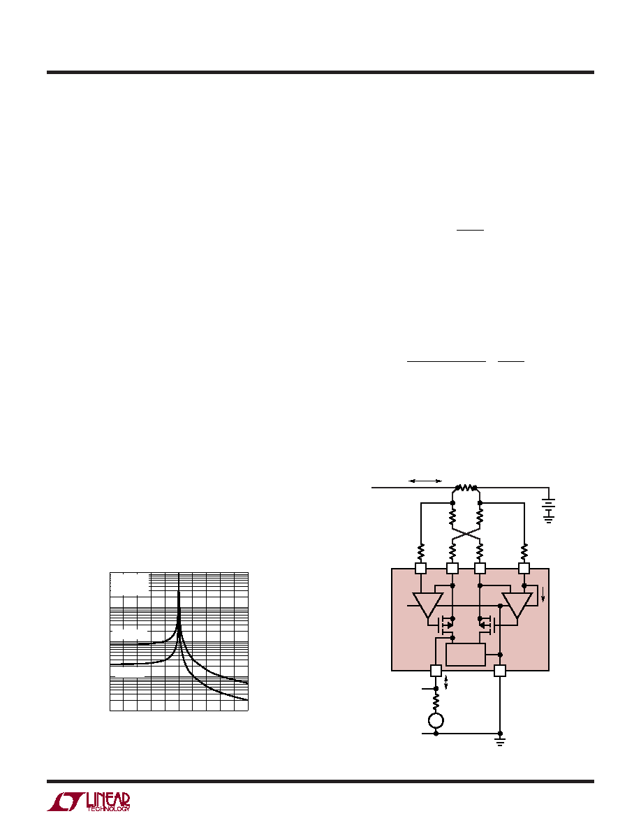
Output Error, EOUT, Due to Trace Resistance
The LTC6104 uses the +INB pin for both the positive “B”
amplier input and the positive supply input for both
ampliers. If trace resistance (RT) become signicant
(Figure 5), this supply current can cause an input offset
error, which can be calculated as follows:
ER
I
R
OUT OFFSET
T
S
OUT
IN
()
=
Trace resistances to the –IN terminals will increase the
effective RIN value, causing a gain error (Figure 5). In ad-
dition, internal device resistance will add approximately
0.3
Ω to RIN.
Gain error equals:
A
R
RR
R
V ERROR
OUT
IN
T
OUT
IN
()
.
–
=
++ 03
Minimizing resistance in the input traces is important and
care should be taken in the PCB layout. Make the trace
short and wide. Kelvin connection to the shunt resistor
pad should be used. Avoid tapping into this signal along
Figure 5. Errors from PCB Traces and Other Parasitic Resistances
VSENSE (mV)
0.1
OUTPUT
ERROR
(%)
1
10
100
–500
–100
100
300
0.01
–300
500
6104 F04
MAXIMUM
TYPICAL
RIN = 100
ROUT = 5k
Figure 4. Output Error vs Input Voltage
+
–
8
7
6
4
+INA
OUT
+
–
VS
IS
VS
A
LTC6104
–INA
–INB
RIN
RT
TO
CHARGER/LOAD
RSENSE
VSENSE +
–
+INB
V–
ILOAD
+
CURRENT
MIRROR
+
–
5
B
ROUT
IOUT
VREF
6104 F05
VOUT
+
–
1
RT
相关PDF资料 |
PDF描述 |
|---|---|
| LSN-0.8/15-D12H | 1-OUTPUT 12 W DC-DC REG PWR SUPPLY MODULE |
| LP3907SQX-JIXI | 1.5 A DUAL SWITCHING CONTROLLER, 2100 kHz SWITCHING FREQ-MAX, QCC24 |
| LT1004IPWRG4-1-2 | 1-OUTPUT TWO TERM VOLTAGE REFERENCE, 1.235 V, PDSO8 |
| LTC2912HDDB-3#PBF | 1-CHANNEL POWER SUPPLY SUPPORT CKT, PDSO8 |
| LK1501-9EPDD | 1-OUTPUT 150 W AC-DC REG PWR SUPPLY MODULE |
相关代理商/技术参数 |
参数描述 |
|---|---|
| LTC6104CMS8#PBF | 功能描述:IC AMP CURRENT SENSE 8-MSOP RoHS:是 类别:集成电路 (IC) >> Linear - Amplifiers - Instrumentation 系列:- 其它有关文件:Automotive Product Guide 产品培训模块:Lead (SnPb) Finish for COTS Obsolescence Mitigation Program 标准包装:1 系列:- 放大器类型:通用 电路数:1 输出类型:满摆幅 转换速率:3 V/µs 增益带宽积:10MHz -3db带宽:- 电流 - 输入偏压:1pA 电压 - 输入偏移:70µV 电流 - 电源:2.5mA 电流 - 输出 / 通道:48mA 电压 - 电源,单路/双路(±):2.7 V ~ 5.5 V,±1.35 V ~ 2.75 V 工作温度:-40°C ~ 125°C 安装类型:表面贴装 封装/外壳:SOT-23-6 供应商设备封装:SOT-6 包装:Digi-Reel® 其它名称:MAX4475AUT#TG16DKR |
| LTC6104CMS8#TRPBF | 功能描述:IC AMP CURRENT SENSE 8-MSOP RoHS:是 类别:集成电路 (IC) >> Linear - Amplifiers - Instrumentation 系列:- 标准包装:1,000 系列:- 放大器类型:电压反馈 电路数:4 输出类型:满摆幅 转换速率:33 V/µs 增益带宽积:20MHz -3db带宽:30MHz 电流 - 输入偏压:2nA 电压 - 输入偏移:3000µV 电流 - 电源:2.5mA 电流 - 输出 / 通道:30mA 电压 - 电源,单路/双路(±):4.5 V ~ 16.5 V,±2.25 V ~ 8.25 V 工作温度:-40°C ~ 85°C 安装类型:表面贴装 封装/外壳:14-SOIC(0.154",3.90mm 宽) 供应商设备封装:14-SOIC 包装:带卷 (TR) |
| LTC6104CMS8PBF | 制造商:Linear Technology 功能描述:Bi-Directional Curr Sense Amp LTC6104 |
| LTC6104HMS8 | 制造商:LINER 制造商全称:Linear Technology 功能描述:High Voltage, High Side, Bi-Directional Current Sense Amplifi er |
| LTC6104HMS8#PBF | 功能描述:IC AMP CURRENT SENSE 8-MSOP RoHS:是 类别:集成电路 (IC) >> Linear - Amplifiers - Instrumentation 系列:- 产品培训模块:Differential Circuit Design Techniques for Communication Applications 标准包装:1 系列:- 放大器类型:RF/IF 差分 电路数:1 输出类型:差分 转换速率:9800 V/µs 增益带宽积:- -3db带宽:2.9GHz 电流 - 输入偏压:3µA 电压 - 输入偏移:- 电流 - 电源:40mA 电流 - 输出 / 通道:- 电压 - 电源,单路/双路(±):3 V ~ 3.6 V 工作温度:-40°C ~ 85°C 安装类型:表面贴装 封装/外壳:16-VQFN 裸露焊盘,CSP 供应商设备封装:16-LFCSP-VQ 包装:剪切带 (CT) 产品目录页面:551 (CN2011-ZH PDF) 其它名称:ADL5561ACPZ-R7CT |
发布紧急采购,3分钟左右您将得到回复。