参数资料
| 型号: | LTC6242CGN#TRPBF |
| 厂商: | Linear Technology |
| 文件页数: | 14/32页 |
| 文件大小: | 0K |
| 描述: | IC OP AMP QUAD R-R 16-SSOP |
| 标准包装: | 2,500 |
| 放大器类型: | 通用 |
| 电路数: | 4 |
| 输出类型: | 满摆幅 |
| 转换速率: | 10 V/µs |
| 增益带宽积: | 18MHz |
| 电流 - 输入偏压: | 0.2pA |
| 电压 - 输入偏移: | 50µV |
| 电流 - 电源: | 1.8mA |
| 电流 - 输出 / 通道: | 30mA |
| 电压 - 电源,单路/双路(±): | 2.8 V ~ 6 V |
| 工作温度: | 0°C ~ 70°C |
| 安装类型: | 表面贴装 |
| 封装/外壳: | 16-SSOP(0.154",3.90mm 宽) |
| 供应商设备封装: | 16-SSOP |
| 包装: | 带卷 (TR) |
第1页第2页第3页第4页第5页第6页第7页第8页第9页第10页第11页第12页第13页当前第14页第15页第16页第17页第18页第19页第20页第21页第22页第23页第24页第25页第26页第27页第28页第29页第30页第31页第32页
LTC6240/LTC6241/LTC6242
21
624012fe
The op amp’s good input offset voltage match and low
input bias current means that the typical differential output
offset voltage is less than 40μV. A noise spectrum plot of
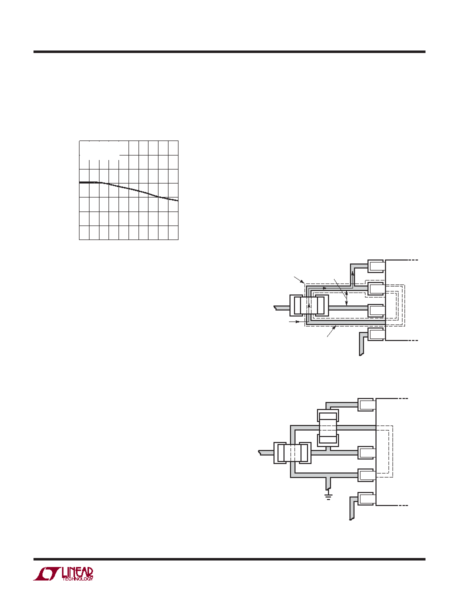
the differential output is shown in Figure 5.
The guard ring should extend as far as necessary to shield
the high impedance signal from any and all leakage paths.
Figure 6 shows the use of a guard ring on the LTC6241 in
a unity gain conguration. In this case the guard ring is
connected to the output and is shielding the high impedance
noninverting input from V–. Figure 7 shows the inverting
gain conguration.
A Digitally Programmable AC Difference Amplier
The LTC6241 congured as a difference amplier, can be
combined with a programmable gain amplier (PGA) to
obtain a low noise high speed programmable difference
amplier. Figure 8 shows the LTC6241 based as a single-
supply AC amplier. One LTC6241 op amp is used at the
circuit’s input as a standard four resistor difference amplier.
Figure 5. Differential Output Noise
Achieving Low Input Bias Current
The DD package is leadless and makes contact to the PCB
beneath the package. Solder ux used during the attach-
ment of the part to the PCB can create leakage current
paths and can degrade the input bias current performance
of the part. All inputs are susceptible because the backside
paddle is connected to V– internally. As the input voltage
changes or if V– changes, a leakage path can be formed
and alter the observed input bias current. For lowest bias
current, use the LTC6240/LTC6241 in the SO-8 and provide
a guard ring around the inputs that are tied to a potential
near the input voltage.
Layout Considerations and a PCB Guard Ring
In high source impedance applications such as pH probes,
photodiodes, strain gauges, et cetera, the low input bias
current of these parts requires a clean board layout to
minimize additional leakage current into a high impedance
signal node. A mere 100GΩ of PC board resistance
between a 5V supply trace and an input trace adds 50pA
of leakage current, far greater then the input bias current
of the operational amplier. A guard ring around the high
impedance input traces driven by a low impedance source
equal to the input voltage prevents such leakage problems.
Figure 6. Sample Layout. Unity Gain Conguration, Using Guard
Ring to Shield High Impedance Input from Board Leakage
Figure 7. Sample Layout. Inverting Gain Conguration, Using
Guard Ring to Shield High Impedance Input from Board Leakage
APPLICATIONS INFORMATION
FREQUENCY (kHz)
020
60
10
40
80
30
70
50
90 100
DIFFERENTIAL
OUTPUT
VOLTAGE
DENSITY
(nV/√
Hz
)
140
60
80
100
120
0
20
40
6241 F05
VS = ±2.5V
TA = 25°C
–3dB BW = 80kHz
LTC6241 S8
R
OUT+
IN–
IN+
V–
LEAKAGE
CURRENT
NO LEAKAGE
CURRENT
GUARD
RING
NO SOLDER MASK
OVER THE GUARD RING
LTC6241 F06
LTC6241 S8
LTC6241 F07
R
OUT+
IN–
IN+
V–
VIN
GND
相关PDF资料 |
PDF描述 |
|---|---|
| LTC6244HVCDD#TRPBF | IC OP AMP DUAL R-R 8-DFN |
| LTC6247CTS8#TRPBF | IC OPAMP RRIO 180MHZ DL TSOT23-8 |
| LTC6253CTS8#TRPBF | IC OPAMP R-R 720MHZ TSOT23-8 |
| LTC6256IKC#TRMPBF | IC OP AMP RRIO DUAL 8UTDFN |
| LTC6410IUD-6#PBF | IC AMP DIFF IF 16-QFN |
相关代理商/技术参数 |
参数描述 |
|---|---|
| LTC6242HGN | 制造商:Linear Technology 功能描述:OP Amp Quad GP R-R O/P 6V 16-Pin SSOP N |
| LTC6242HGN#PBF | 功能描述:IC OP AMP QUAD R-R 16-SSOP RoHS:是 类别:集成电路 (IC) >> Linear - Amplifiers - Instrumentation 系列:- 标准包装:100 系列:- 放大器类型:通用 电路数:1 输出类型:- 转换速率:0.2 V/µs 增益带宽积:- -3db带宽:- 电流 - 输入偏压:100pA 电压 - 输入偏移:30µV 电流 - 电源:380µA 电流 - 输出 / 通道:- 电压 - 电源,单路/双路(±):±2 V ~ 18 V 工作温度:0°C ~ 70°C 安装类型:表面贴装 封装/外壳:8-SOIC(0.154",3.90mm 宽) 供应商设备封装:8-SO 包装:管件 |
| LTC6242HGN#TRPBF | 功能描述:IC OP AMP QUAD R-R 16-SSOP RoHS:是 类别:集成电路 (IC) >> Linear - Amplifiers - Instrumentation 系列:- 标准包装:100 系列:- 放大器类型:通用 电路数:1 输出类型:- 转换速率:0.2 V/µs 增益带宽积:- -3db带宽:- 电流 - 输入偏压:100pA 电压 - 输入偏移:30µV 电流 - 电源:380µA 电流 - 输出 / 通道:- 电压 - 电源,单路/双路(±):±2 V ~ 18 V 工作温度:0°C ~ 70°C 安装类型:表面贴装 封装/外壳:8-SOIC(0.154",3.90mm 宽) 供应商设备封装:8-SO 包装:管件 |
| LTC6242HVCDHC | 制造商:Linear Technology 功能描述:OP Amp Quad GP R-R O/P ±5.5V/11V 16-Pin DFN EP |
| LTC6242HVCDHC#PBF | 功能描述:IC OP AMP QUAD R-R 16-DFN RoHS:是 类别:集成电路 (IC) >> Linear - Amplifiers - Instrumentation 系列:- 标准包装:50 系列:- 放大器类型:J-FET 电路数:2 输出类型:- 转换速率:3.5 V/µs 增益带宽积:1MHz -3db带宽:- 电流 - 输入偏压:30pA 电压 - 输入偏移:2000µV 电流 - 电源:200µA 电流 - 输出 / 通道:- 电压 - 电源,单路/双路(±):7 V ~ 36 V,±3.5 V ~ 18 V 工作温度:0°C ~ 70°C 安装类型:通孔 封装/外壳:8-DIP(0.300",7.62mm) 供应商设备封装:8-PDIP 包装:管件 |
发布紧急采购,3分钟左右您将得到回复。