- 您现在的位置:买卖IC网 > PDF目录80228 > LTC6360IDD#PBF (LINEAR TECHNOLOGY CORP) SPECIALTY ANALOG CIRCUIT, PDSO8 PDF资料下载
参数资料
| 型号: | LTC6360IDD#PBF |
| 厂商: | LINEAR TECHNOLOGY CORP |
| 元件分类: | 模拟信号调理 |
| 英文描述: | SPECIALTY ANALOG CIRCUIT, PDSO8 |
| 封装: | 3 X 3 MM, LEAD FREE, PLASTIC, M0-229WEED-1, DFN-8 |
| 文件页数: | 5/24页 |
| 文件大小: | 514K |
| 代理商: | LTC6360IDD#PBF |
LTC6360
13
6360f
applicaTions inForMaTion
Input bias current induced DC voltage offsets can be
minimized by matching the parallel impedance of RF and
RG to the source impedance, RS. For example, in the
typical application when the amplifier is configured as a
unity gain buffer, choosing RF equal to RS will minimize
the offset. Since nonzero values of RFwillcontributetothe
total output noise, RF may be bypassed with a capacitor
to reduce the noise bandwidth.
Input Protection
Back-to-back diodes (D1 and D2 in Figure 5) are included
between +IN and –IN to protect the input devices. The
inputs do not have internal resistors in series with the
input transistors, a technique often used to protect the
input transistors from excessive current flow during an
overdrive condition. Adding series input resistors would
significantlydegradethelownoiseperformance.Therefore,
if the voltage across the amplifier’s inputs is allowed to
exceed ±0.7V, steady state current conducted through the
protection diodes should be externally limited to ±10mA.
The input diodes are rugged enough to handle transient
currentsduetoamplifierslewrateoverdriveormomentary
clipping without protection resistors.
Driving the input signal sufficiently beyond the specified
input common mode voltage range will cause the input
transistorstosaturate.Whensaturationoccurs,theampli-
fier loses a stage of phase inversion and the output will
begin to invert. Diode D1 or D2 (Figure 5) forward biases
andholdstheoutputwithinadiodedropoftheinputsignal.
To avoid this inversion, limit the input drive to within the
specified input common mode range.
ESD
The LTC6360 has ESD protection diodes on all inputs
and outputs. The diodes are reverse biased during nor-
mal operation. If the input pins are driven beyond either
supply, large currents will flow through these diodes. If
the current is transient and limited to 10mA or less, no
damage to the device will occur.
On-Chip Charge Pump
A low noise on-chip charge pump generates a small nega-
tive voltage that is used to bias the output stage of the
amplifier, enabling output swing below 0V. The charge
pump output voltage is typically –0.6V. Several design
techniques have been used to lower the ripple present
at OUT due to the switching action of the charge pump.
The charge pump output is made available via the CPO
pin, and the amplifier’s charge pump input at the CPI pin.
This allows additional external filtering via a capacitor
connected from CPI to GND.
The charge pump operates at a nominal frequency of
10MHz.TheoutputvoltageatCPOwillhavesmallfrequency
components at multiples of 5MHz. These components
are further reduced by the PSRR of the amplifier’s out-
put stage. The amplitude of the fundamental component
at the OUT pin is typically 1VRMS with a 0.1F bypass
capacitor at CPI.
Conventionally, a two chip solution is chosen to provide
output swing to true zero on a single supply: one ampli-
fier and an inverting charge pump to provide a negative
rail. Compared to a two chip solution, the LTC6360 offers
several advantages: a more compact layout with lower
part count, lower output ripple, less EMI and lower power.
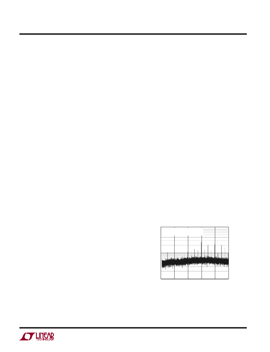
Figure 6 shows the ripple voltage spectrum at the output,
VOUT, with a 0.1F external CPI bypass capacitor.
Figure 6. Output Ripple Voltage
FREQUENCY (MHz)
V OUT
(V
RMS
)
1
0.1
10
100
80
60
40
20
0
6360 F06
INPUT GROUNDED
0.1F CPI BYPASS CAPACITOR
相关PDF资料 |
PDF描述 |
|---|---|
| LS1301-9EPDDTB1 | 1-OUTPUT 100 W AC-DC REG PWR SUPPLY MODULE |
| LT1243MJ8 | 1 A SWITCHING CONTROLLER, 500 kHz SWITCHING FREQ-MAX, CDIP8 |
| LT1019MS-4.5 | 1-OUTPUT THREE TERM VOLTAGE REFERENCE, 4.5 V, PDSO |
| LS1301-7RD3TB1 | 1-OUTPUT AC-DC REG PWR SUPPLY MODULE |
| LS1301-9RD1TB1 | 1-OUTPUT AC-DC REG PWR SUPPLY MODULE |
相关代理商/技术参数 |
参数描述 |
|---|---|
| LTC6360IMS8E#PBF | 功能描述:IC ADC DRIVER TRUE ZERO 8MSOP RoHS:是 类别:集成电路 (IC) >> 线性 - 放大器 - 专用 系列:- 产品培训模块:Lead (SnPb) Finish for COTS Obsolescence Mitigation Program 标准包装:60 系列:- 类型:可变增益放大器 应用:CATV 安装类型:表面贴装 封装/外壳:20-WQFN 裸露焊盘 供应商设备封装:20-TQFN-EP(5x5) 包装:托盘 |
| LTC6360IMS8E#TRPBF | 功能描述:IC ADC DRIVER TRUE ZERO 8MSOP RoHS:是 类别:集成电路 (IC) >> 线性 - 放大器 - 专用 系列:- 产品培训模块:Lead (SnPb) Finish for COTS Obsolescence Mitigation Program 标准包装:60 系列:- 类型:可变增益放大器 应用:CATV 安装类型:表面贴装 封装/外壳:20-WQFN 裸露焊盘 供应商设备封装:20-TQFN-EP(5x5) 包装:托盘 |
| LTC6362 | 制造商:LINER 制造商全称:Linear Technology 功能描述:Precision, Low Power Rail-to-Rail Input/Output |
| LTC6362CDD#PBF | 功能描述:IC OPAMP DIFFERENTIAL R-R 8DFN RoHS:是 类别:集成电路 (IC) >> Linear - Amplifiers - Instrumentation 系列:- 标准包装:1,000 系列:- 放大器类型:电压反馈 电路数:4 输出类型:满摆幅 转换速率:33 V/µs 增益带宽积:20MHz -3db带宽:30MHz 电流 - 输入偏压:2nA 电压 - 输入偏移:3000µV 电流 - 电源:2.5mA 电流 - 输出 / 通道:30mA 电压 - 电源,单路/双路(±):4.5 V ~ 16.5 V,±2.25 V ~ 8.25 V 工作温度:-40°C ~ 85°C 安装类型:表面贴装 封装/外壳:14-SOIC(0.154",3.90mm 宽) 供应商设备封装:14-SOIC 包装:带卷 (TR) |
| LTC6362CDD#TRPBF | 功能描述:IC OPAMP DIFFERENTIAL R-R 8DFN RoHS:是 类别:集成电路 (IC) >> Linear - Amplifiers - Instrumentation 系列:- 标准包装:1,000 系列:- 放大器类型:电压反馈 电路数:4 输出类型:满摆幅 转换速率:33 V/µs 增益带宽积:20MHz -3db带宽:30MHz 电流 - 输入偏压:2nA 电压 - 输入偏移:3000µV 电流 - 电源:2.5mA 电流 - 输出 / 通道:30mA 电压 - 电源,单路/双路(±):4.5 V ~ 16.5 V,±2.25 V ~ 8.25 V 工作温度:-40°C ~ 85°C 安装类型:表面贴装 封装/外壳:14-SOIC(0.154",3.90mm 宽) 供应商设备封装:14-SOIC 包装:带卷 (TR) |
发布紧急采购,3分钟左右您将得到回复。