- 您现在的位置:买卖IC网 > PDF目录80228 > LTC6360IDD#PBF (LINEAR TECHNOLOGY CORP) SPECIALTY ANALOG CIRCUIT, PDSO8 PDF资料下载
参数资料
| 型号: | LTC6360IDD#PBF |
| 厂商: | LINEAR TECHNOLOGY CORP |
| 元件分类: | 模拟信号调理 |
| 英文描述: | SPECIALTY ANALOG CIRCUIT, PDSO8 |
| 封装: | 3 X 3 MM, LEAD FREE, PLASTIC, M0-229WEED-1, DFN-8 |
| 文件页数: | 6/24页 |
| 文件大小: | 514K |
| 代理商: | LTC6360IDD#PBF |
LTC6360
14
6360f
applicaTions inForMaTion
The charge pump is capable of sinking up to 4.5mA of
DC current with a typical DC output impedance of 30Ω. If
more current is demanded of the charge pump, the volt-
age at CPO will collapse towards 0V. A diode connected
from CPO to GND limits the CPO node from being pulled
above ground by more than one diode drop.
Transient currents are absorbed by the filter capacitors
from CPO/CPI to GND. Care should be taken in selecting
the filter capacitors such that there is minimum ripple
voltage and droop during peak transient current demand.
Using multiple small surface mount capacitors is ad-
vised, with each capacitor covering a portion of the total
frequency range.
Slew Rate and Full Power Bandwidth
Additional consideration needs to be paid to the current
demanded of the charge pump. When driving a capaci-
tive load, the LTC6360 will exhibit a clipped distortion
characteristic at a lower frequency than where slew rate
limited distortion would occur. In contrast to a traditional
amplifier, where the full power bandwidth is determined
from the amplifier’s slew rate, when driving capacitive
loads, the full power bandwidth of the LTC6360 will be
limited by the charge pump sinking capability.
Theaveragecurrentsunkbythechargepumpwhendriving
a capacitive load can be approximated as:
ICP(AVG) = 2VP CFILT f + 1mA
(1)
where VP and f are the amplitude and frequency of the
driven signal respectively.
Themaximumfrequencythatthechargepumpcansupport
while maintaining the CPO pin below –0.4V is:
fFPBW = (ICP(MAX) – 1mA)/(2VP CFILT)
(2)
whereICP(MAX)isgiveninthespecificationtable.Full-scale
signals beyond this frequency will cause the charge pump
to collapse towards 0V, limiting the output amplitude and
causing distortion.
Output Compensation
The LTC6360 is internally compensated to be gain of 5
stable. Lower gains require an external RC network at
the output to provide compensation. The amplifier has
been decompensated to provide the highest possible
gain-bandwidth with a typical RC load of 10Ω in series
with 330pF. The extra gain-bandwidth obtained serves to
reducedistortionoverawiderbandwidth.Sinceanexternal
RC filter network is desired in most ADC applications, the
decompensationistransparentinthesecasesandactually
serves to improve distortion performance.
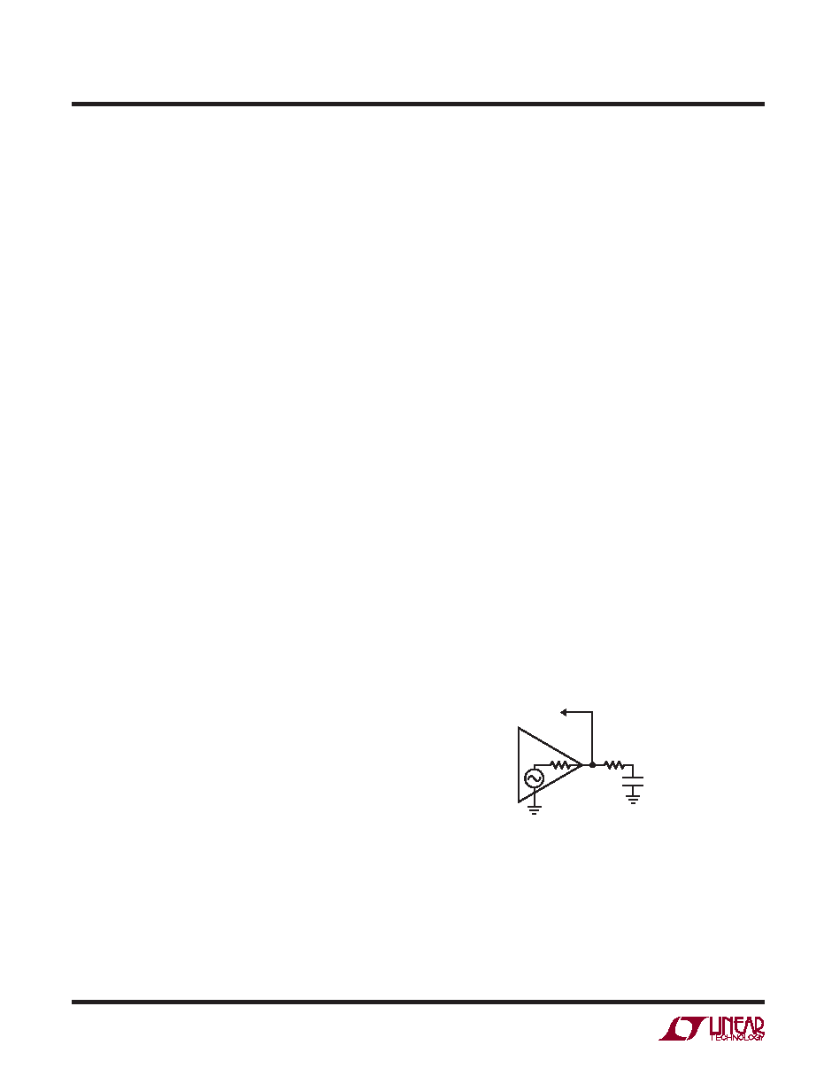
The RC network at the output contributes a pole-zero pair
that reduces the loop gain above the pole frequency. The
simplified circuit model at high frequencies is shown in
Figure 7. At high frequencies, the open-loop output imped-
ance of the amplifier can be represented by an equivalent
resistor, ro, of 45Ω.
The pole frequency is:
fP = 1/(2π(RFILT + ro)CFILT)
(3)
The zero frequency is:
fZ = 1/(2πRFILTCFILT)
(4)
which is also the –3dB bandwidth of the filter formed by
RFILT and CFILT. The zero-pole ratio is given by:
fZ/fP = 1 + ro/RFILT
(5)
Figure 7. Pole-Zero Introduced by RC Network at Output
6360 F07
TO FEEDBACK
NETWORK
AMPLIFIER
fZ = 1/[2πRFILTCFILT]
f
ρ = 1/[2π(RFILT + ro)CFILT]
OUT
RFILT
CFILT
ro
VO
+
–
相关PDF资料 |
PDF描述 |
|---|---|
| LS1301-9EPDDTB1 | 1-OUTPUT 100 W AC-DC REG PWR SUPPLY MODULE |
| LT1243MJ8 | 1 A SWITCHING CONTROLLER, 500 kHz SWITCHING FREQ-MAX, CDIP8 |
| LT1019MS-4.5 | 1-OUTPUT THREE TERM VOLTAGE REFERENCE, 4.5 V, PDSO |
| LS1301-7RD3TB1 | 1-OUTPUT AC-DC REG PWR SUPPLY MODULE |
| LS1301-9RD1TB1 | 1-OUTPUT AC-DC REG PWR SUPPLY MODULE |
相关代理商/技术参数 |
参数描述 |
|---|---|
| LTC6360IMS8E#PBF | 功能描述:IC ADC DRIVER TRUE ZERO 8MSOP RoHS:是 类别:集成电路 (IC) >> 线性 - 放大器 - 专用 系列:- 产品培训模块:Lead (SnPb) Finish for COTS Obsolescence Mitigation Program 标准包装:60 系列:- 类型:可变增益放大器 应用:CATV 安装类型:表面贴装 封装/外壳:20-WQFN 裸露焊盘 供应商设备封装:20-TQFN-EP(5x5) 包装:托盘 |
| LTC6360IMS8E#TRPBF | 功能描述:IC ADC DRIVER TRUE ZERO 8MSOP RoHS:是 类别:集成电路 (IC) >> 线性 - 放大器 - 专用 系列:- 产品培训模块:Lead (SnPb) Finish for COTS Obsolescence Mitigation Program 标准包装:60 系列:- 类型:可变增益放大器 应用:CATV 安装类型:表面贴装 封装/外壳:20-WQFN 裸露焊盘 供应商设备封装:20-TQFN-EP(5x5) 包装:托盘 |
| LTC6362 | 制造商:LINER 制造商全称:Linear Technology 功能描述:Precision, Low Power Rail-to-Rail Input/Output |
| LTC6362CDD#PBF | 功能描述:IC OPAMP DIFFERENTIAL R-R 8DFN RoHS:是 类别:集成电路 (IC) >> Linear - Amplifiers - Instrumentation 系列:- 标准包装:1,000 系列:- 放大器类型:电压反馈 电路数:4 输出类型:满摆幅 转换速率:33 V/µs 增益带宽积:20MHz -3db带宽:30MHz 电流 - 输入偏压:2nA 电压 - 输入偏移:3000µV 电流 - 电源:2.5mA 电流 - 输出 / 通道:30mA 电压 - 电源,单路/双路(±):4.5 V ~ 16.5 V,±2.25 V ~ 8.25 V 工作温度:-40°C ~ 85°C 安装类型:表面贴装 封装/外壳:14-SOIC(0.154",3.90mm 宽) 供应商设备封装:14-SOIC 包装:带卷 (TR) |
| LTC6362CDD#TRPBF | 功能描述:IC OPAMP DIFFERENTIAL R-R 8DFN RoHS:是 类别:集成电路 (IC) >> Linear - Amplifiers - Instrumentation 系列:- 标准包装:1,000 系列:- 放大器类型:电压反馈 电路数:4 输出类型:满摆幅 转换速率:33 V/µs 增益带宽积:20MHz -3db带宽:30MHz 电流 - 输入偏压:2nA 电压 - 输入偏移:3000µV 电流 - 电源:2.5mA 电流 - 输出 / 通道:30mA 电压 - 电源,单路/双路(±):4.5 V ~ 16.5 V,±2.25 V ~ 8.25 V 工作温度:-40°C ~ 85°C 安装类型:表面贴装 封装/外壳:14-SOIC(0.154",3.90mm 宽) 供应商设备封装:14-SOIC 包装:带卷 (TR) |
发布紧急采购,3分钟左右您将得到回复。