- 您现在的位置:买卖IC网 > PDF目录2156 > LTC6412CUF#TRPBF (Linear Technology)IC VGA ANLG-CNTRL 31DB 24-QFN PDF资料下载
参数资料
| 型号: | LTC6412CUF#TRPBF |
| 厂商: | Linear Technology |
| 文件页数: | 8/24页 |
| 文件大小: | 0K |
| 描述: | IC VGA ANLG-CNTRL 31DB 24-QFN |
| 标准包装: | 2,500 |
| 放大器类型: | 可变增益 |
| 电路数: | 1 |
| 输出类型: | 差分 |
| -3db带宽: | 800MHz |
| 电流 - 电源: | 110mA |
| 电流 - 输出 / 通道: | 70mA |
| 电压 - 电源,单路/双路(±): | 3 V ~ 3.6 V |
| 工作温度: | 0°C ~ 70°C |
| 安装类型: | 表面贴装 |
| 封装/外壳: | 24-WFQFN 裸露焊盘 |
| 供应商设备封装: | 24-QFN 裸露焊盘(4x4) |
| 包装: | 带卷 (TR) |
LTC6412
16
6412fa
APPLICATIONS INFORMATION
grounding and supply decoupling. Failure to provide low
impedance supply and ground at high frequencies can
cause oscillations and increased distortion.
Enable/Shutdown
Both the EN pin and SHDN pin are self-biased to VCCthrough
their respective 100k pull-up resistors, so the default
open-pin state is powered on with the output amplier
signal path disabled. Pulling the EN pin low completes
the signal path from the attenuator ladder through the
output amplier. The EN pin essentially provides a fast
muting function while the SHDN pin provides slower
power on/off function.
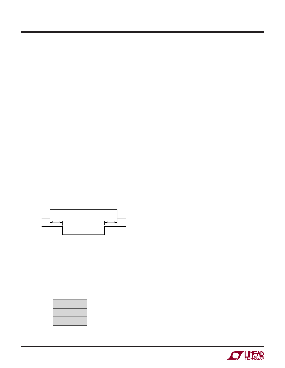
For applications requiring the SHDN function, it is
recommended that the output amplier signal path be
disabled with a high EN voltage before transitioning the
SHDN signal. When enabling the amplier, allow at least
5ms dwell time between the rising SHDN transition and the
falling EN transition to avoid non-monotonic output signal
behavior though the VGA. The opposite delay sequence
is recommended for the falling SHDN transition, but this
is less critical as the output signal amplitude will drop
abruptly regardless of the EN pin.
SHDN
EN
tDWELL
6412 AI01
Layout/Grounding
The high frequency performance of the LTC6412 requires
special attention to proper RF grounding, bias decoupling
and termination. The recommended PCB stack-up for a
4-layer board is shown below for 1oz copper clad FR-4
laminate with a relative dielectric constant,
εr = 4.2-4.5
at 1GHz.
METAL 1
METAL 2
METAL 3
METAL 4
RF SIGNAL
FR4 12-18 MILS
FR4 20-30 MILS
FR4 NOT CRITICAL
GROUND PLANE
POWER PLANE
GND AND LF SIGNAL
6412 AI02
The topside metal and silkscreen drawings for Test Circuit A
illustrate the recommended decoupling capacitor place-
ment, signal routing and grounding. Ground vias directly
beneaththeExposedPadarecritical;useasmanyaspossible.
Ground vias to the other ground pins are less critical.
ESD
The LTC6412 is protected with reverse-biased ESD diodes
on all I/O pins. If any I/O pin is forced one diode drop above
the positive supply or one diode drop below the negative
supply, then large currents may ow through the diodes.
No damage to the devices will occur if the current is kept
below 10 mA. The +OUT/–OUT pins have additional series
diodes to the positive supply and can sustain approximately
2V overshoot above the positive supply before conducting
appreciable currents.
Signal Compression Characteristics
The graph entitled, Input and Output P1dB, illustrates
an important characteristic of the LTC6412 VGA. At gain
settings above –5dB, the output amplier limits the linear
power handling capability, but at gain settings below
–5dB, the input attenuator ladder limits the linear power
handling capability. The linear input power limitations at
minimum gain do not affect the overall performance of
a signal chain if the preceding mixer or amplier stage
exhibits an OP1dB < 19dBm and an OIP3 < 50dBm.
Test Circuits
The fully-differential nature of the LTC6412 design requires
two test circuits to generate the performance information
presented in this data sheet.
Test Circuit A is DC1464A, a 2-port demonstration circuit
with input/output balun transformers to allow for direct
connection to a 2-port network analyzer or other single-
ended 50Ω test system. The balun transformers limit the
high and low frequency performance of the LTC6412 but
allow for simple and reasonably accurate measurements
from 70MHz to 380MHz. The gain control signal is supplied
to either of the VG turrets for DC control measurements
or through the VGAIN SMA connector for transient control
signal measurements. Clip leads to the gain control turrets
are susceptible to noise pickup and should be lowpass
相关PDF资料 |
PDF描述 |
|---|---|
| LTC6416IDDB#TRPBF | IC DIFF 16BIT BUFFER 10-DFN |
| LTC6800HDD#TRPBF | IC OP AMP INSTR R-R I/O 8-DFN |
| LTC6910-2HTS8#TRPBF | IC PGA DIGITAL R-R I/O TSOT23-8 |
| LTC6911HMS-2#TRPBF | IC PGA DIGITAL R-R DUAL 10MSOP |
| LTC6912CDE-1#TRPBF | IC PGA DIGITAL R-R DUAL 12-DFN |
相关代理商/技术参数 |
参数描述 |
|---|---|
| LTC6412IUF | 制造商:LINER 制造商全称:Linear Technology 功能描述:800MHz, 31dB Range Analog-Controlled VGA |
| LTC6412IUF#PBF | 功能描述:IC VGA ANLG-CNTRL 31DB 24-QFN RoHS:是 类别:集成电路 (IC) >> Linear - Amplifiers - Instrumentation 系列:- 标准包装:150 系列:- 放大器类型:音频 电路数:2 输出类型:- 转换速率:5 V/µs 增益带宽积:12MHz -3db带宽:- 电流 - 输入偏压:100nA 电压 - 输入偏移:500µV 电流 - 电源:6mA 电流 - 输出 / 通道:50mA 电压 - 电源,单路/双路(±):4 V ~ 32 V,±2 V ~ 16 V 工作温度:-40°C ~ 85°C 安装类型:表面贴装 封装/外壳:8-TSSOP(0.173",4.40mm 宽) 供应商设备封装:8-TSSOP 包装:管件 |
| LTC6412IUF#TRPBF | 功能描述:IC VGA ANLG-CNTRL 31DB 24-QFN RoHS:是 类别:集成电路 (IC) >> Linear - Amplifiers - Instrumentation 系列:- 标准包装:150 系列:- 放大器类型:音频 电路数:2 输出类型:- 转换速率:5 V/µs 增益带宽积:12MHz -3db带宽:- 电流 - 输入偏压:100nA 电压 - 输入偏移:500µV 电流 - 电源:6mA 电流 - 输出 / 通道:50mA 电压 - 电源,单路/双路(±):4 V ~ 32 V,±2 V ~ 16 V 工作温度:-40°C ~ 85°C 安装类型:表面贴装 封装/外壳:8-TSSOP(0.173",4.40mm 宽) 供应商设备封装:8-TSSOP 包装:管件 |
| LTC6412IUFPBF | 制造商:LINER 制造商全称:Linear Technology 功能描述:800MHz, 31dB Range Analog-Controlled VGA |
| LTC6412IUFTRPBF | 制造商:LINER 制造商全称:Linear Technology 功能描述:800MHz, 31dB Range Analog-Controlled VGA |
发布紧急采购,3分钟左右您将得到回复。