参数资料
| 型号: | LTC6416IDDB#TRPBF |
| 厂商: | Linear Technology |
| 文件页数: | 17/20页 |
| 文件大小: | 0K |
| 描述: | IC DIFF 16BIT BUFFER 10-DFN |
| 标准包装: | 2,500 |
| 放大器类型: | 缓冲器 |
| 电路数: | 1 |
| 输出类型: | 差分 |
| 转换速率: | 3400 V/µs |
| -3db带宽: | 2GHz |
| 电流 - 输入偏压: | 5µA |
| 电压 - 输入偏移: | 500µV |
| 电流 - 电源: | 42mA |
| 电流 - 输出 / 通道: | 20mA |
| 电压 - 电源,单路/双路(±): | 2.7 V ~ 3.9 V,±1.35 V ~ 1.95 V |
| 工作温度: | -40°C ~ 85°C |
| 安装类型: | 表面贴装 |
| 封装/外壳: | 10-WFDFN 裸露焊盘 |
| 供应商设备封装: | 10-DFN-EP(3x2) |
| 包装: | 带卷 (TR) |
LTC6416
6
6416f
Note 1: Stresses beyond those listed under Absolute Maximum Ratings
may cause permanent damage to the device. Exposure to any Absolute
Maximum Rating condition for extended periods may affect device
reliability and lifetime.
Note 2: The LTC6416C/LTC6416I is guaranteed functional over the
operating temperature range of –40°C to 85°C.
Note 3: The LTC6416C is guaranteed to meet specied performance from
0°C to 70°C. It is designed, characterized and expected to meet specied
performance from –40°C and 85°C but is not tested or QA sampled
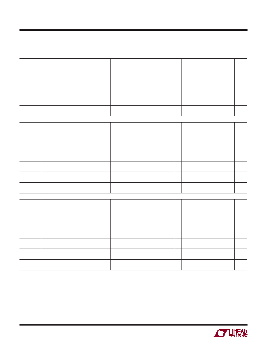
SYMBOL
PARAMETER
CONDITIONS
MIN
TYP
MAX
UNITS
HD3
Third Harmonic Distortion
V+ = 3.3V, VCM = 1.05V, VOUTDIFF = 2VP-P
V+ = 3.3V, VCM = 1.25V, VOUTDIFF = 2VP-P
V+ = 3.6V, VCM = 1.05V, VOUTDIFF = 2VP-P
V+ = 3.6V, VCM = 1.25V, VOUTDIFF = 2VP-P
–73
–60
–94.5
–83
dBc
IM3
Output Third Order Intermodulation
Distortion
V+ = 3.3V, VCM = 1.05V, VOUTDIFF = 2VP-P
V+ = 3.6V, VCM = 1.25V, VOUTDIFF = 2VP-P
–76.5
–86
dBc
OIP3
Output Third Order Intercept (Equivalent)
(Note 5)
V+ = 3.3V, VCM = 1.05V, VOUTDIFF = 2VP-P
V+ = 3.6V, VCM = 1.25V, VOUTDIFF = 2VP-P
42.25
47
dBm
P1dB
Output 1dB Compression Point (Equivalent)
(Note 5)
V+ = 3.6V, VCM = 1.25V
14.1
dBm
140MHz Signal
HD2
Second Harmonic Distortion
V+ = 3.3V, VCM = 1.05V, VOUTDIFF = 2VP-P
V+ = 3.3V, VCM = 1.25V, VOUTDIFF = 2VP-P
V+ = 3.6V, VCM = 1.05V, VOUTDIFF = 2VP-P
V+ = 3.6V, VCM = 1.25V, VOUTDIFF = 2VP-P
–79.5
–75.5
–73
–81
dBc
HD3
Third Harmonic Distortion
V+ = 3.3V, VCM = 1.05V, VOUTDIFF = 2VP-P
V+ = 3.3V, VCM = 1.25V, VOUTDIFF = 2VP-P
V+ = 3.6V, VCM = 1.05V, VOUTDIFF = 2VP-P
V+ = 3.6V, VCM = 1.25V, VOUTDIFF = 2VP-P
–64
–55
–70
–72
dBc
IM3
Output Third Order Intermodulation
Distortion
V+ = 3.3V, VCM = 1.05V, VOUTDIFF = 2VP-P
V+ = 3.6V, VCM = 1.25V, VOUTDIFF = 2VP-P
–75
–84.5
dBc
OIP3
Output Third Order Intercept (Equivalent)
(Note 5)
V+ = 3.3V, VCM = 1.05V, VOUTDIFF = 2VP-P
V+ = 3.6V, VCM = 1.25V, VOUTDIFF = 2VP-P
41.5
46.25
dBm
P1dB
Output 1dB Compression Point (Equivalent)
(Note 5)
V+ = 3.6V, VCM = 1.25V
14.1
dBm
300MHz Signal
HD2
Second Harmonic Distortion
V+ = 3.3V, VCM = 1.05V, VOUTDIFF = 2VP-P
V+ = 3.3V, VCM = 1.25V, VOUTDIFF = 2VP-P
V+ = 3.6V, VCM = 1.05V, VOUTDIFF = 2VP-P
V+ = 3.6V, VCM = 1.25V, VOUTDIFF = 2VP-P
–75
–65
–69.5
–74
dBc
HD3
Third Harmonic Distortion
V+ = 3.3V, VCM = 1.05V, VOUTDIFF = 2VP-P
V+ = 3.3V, VCM = 1.25V, VOUTDIFF = 2VP-P
V+ = 3.6V, VCM = 1.05V, VOUTDIFF = 2VP-P
V+ = 3.6V, VCM = 1.25V, VOUTDIFF = 2VP-P
–59
–51.5
–63
–67.5
dBc
IM3
Output Third Order Intermodulation
Distortion
V+ = 3.3V, VCM = 1.05V, VOUTDIFF = 2VP-P
V+ = 3.6V, VCM = 1.25V, VOUTDIFF = 2VP-P
–68.5
–72.5
–64
dBc
OIP3
Output Third Order Intercept (Equivalent)
(Note 5)
V+ = 3.3V, VCM = 1.05V, VOUTDIFF = 2VP-P
V+ = 3.6V, VCM = 1.25V, VOUTDIFF = 2VP-P
36
38.25
40.25
dBm
P1dB
Output 1dB Compression Point (Equivalent)
(Note 5)
V+ = 3.6V, VCM = 1.25V
12.9
dBm
AC ELECTRICAL CHARACTERISTICS The l denotes the specications which apply over the full operating
temperature range, otherwise specications are at TA = 25°C. V+ = 3.3V and 3.6V unless otherwise noted, GND = 0V, No RLOAD,
CLOAD = 6pF. VCM = 1.25V, CLHI = VCC, CLLO = 0V unless otherwise noted. VINCM is dened as (IN+ + IN–)/2. VOUTCM is dened as
(OUT+ + OUT–)/2. VINDIFF is dened as (IN+ – IN–). VOUTDIFF is dened as (OUT+ – OUT–). See DC test circuit schematic.
at these temperatures. The LT6416I is guaranteed to meet specied
performance from –40°C to 85°C.
Note 4: This parameter is pulse tested.
Note 5: Since the LTC6416 is a voltage-output buffer, a resistive load is not
required when driving an AD converter. Therefore, typical output power is very
small. In order to compare the LTC6416 with ampliers that require a 50Ω
output load, the LTC6416 output voltage swing driving a given RL is converted
to OIP3 and P1dB as if it were driving a 50Ω load. Using this modied
convention, 2VP-P is by denition equal to 10dBm, regardless of actual RL.
相关PDF资料 |
PDF描述 |
|---|---|
| LTC6800HDD#TRPBF | IC OP AMP INSTR R-R I/O 8-DFN |
| LTC6910-2HTS8#TRPBF | IC PGA DIGITAL R-R I/O TSOT23-8 |
| LTC6911HMS-2#TRPBF | IC PGA DIGITAL R-R DUAL 10MSOP |
| LTC6912CDE-1#TRPBF | IC PGA DIGITAL R-R DUAL 12-DFN |
| LTC6915IGN#TRPBF | IC PGA DIGITAL PREC 0DRFT 16SSOP |
相关代理商/技术参数 |
参数描述 |
|---|---|
| LTC6417 | 制造商:LINER 制造商全称:Linear Technology 功能描述:50?? Gain Block IF Amplifier n 20MHz to 1700MHz Bandwidth |
| LTC6417CUDC#PBF | 功能描述:IC DIFF 16BIT BUFFER 20-QFN RoHS:是 类别:集成电路 (IC) >> Linear - Amplifiers - Instrumentation 系列:- 标准包装:50 系列:- 放大器类型:J-FET 电路数:2 输出类型:- 转换速率:3.5 V/µs 增益带宽积:1MHz -3db带宽:- 电流 - 输入偏压:30pA 电压 - 输入偏移:2000µV 电流 - 电源:200µA 电流 - 输出 / 通道:- 电压 - 电源,单路/双路(±):7 V ~ 36 V,±3.5 V ~ 18 V 工作温度:0°C ~ 70°C 安装类型:通孔 封装/外壳:8-DIP(0.300",7.62mm) 供应商设备封装:8-PDIP 包装:管件 |
| LTC6417CUDC#TRPBF | 功能描述:IC DIFF 16BIT BUFFER 20-QFN RoHS:是 类别:集成电路 (IC) >> Linear - Amplifiers - Instrumentation 系列:- 标准包装:50 系列:- 放大器类型:J-FET 电路数:2 输出类型:- 转换速率:13 V/µs 增益带宽积:3MHz -3db带宽:- 电流 - 输入偏压:65pA 电压 - 输入偏移:3000µV 电流 - 电源:1.4mA 电流 - 输出 / 通道:- 电压 - 电源,单路/双路(±):7 V ~ 36 V,±3.5 V ~ 18 V 工作温度:-40°C ~ 85°C 安装类型:通孔 封装/外壳:8-DIP(0.300",7.62mm) 供应商设备封装:8-PDIP 包装:管件 |
| LTC6417IUDC#PBF | 功能描述:IC DIFF 16BIT BUFFER 20-QFN RoHS:是 类别:集成电路 (IC) >> Linear - Amplifiers - Instrumentation 系列:- 标准包装:50 系列:- 放大器类型:J-FET 电路数:2 输出类型:- 转换速率:13 V/µs 增益带宽积:3MHz -3db带宽:- 电流 - 输入偏压:65pA 电压 - 输入偏移:3000µV 电流 - 电源:1.4mA 电流 - 输出 / 通道:- 电压 - 电源,单路/双路(±):7 V ~ 36 V,±3.5 V ~ 18 V 工作温度:-40°C ~ 85°C 安装类型:通孔 封装/外壳:8-DIP(0.300",7.62mm) 供应商设备封装:8-PDIP 包装:管件 |
| LTC6417IUDC#TRPBF | 功能描述:IC DIFF 16BIT BUFFER 20-QFN RoHS:是 类别:集成电路 (IC) >> Linear - Amplifiers - Instrumentation 系列:- 标准包装:50 系列:- 放大器类型:J-FET 电路数:2 输出类型:- 转换速率:13 V/µs 增益带宽积:3MHz -3db带宽:- 电流 - 输入偏压:65pA 电压 - 输入偏移:3000µV 电流 - 电源:1.4mA 电流 - 输出 / 通道:- 电压 - 电源,单路/双路(±):7 V ~ 36 V,±3.5 V ~ 18 V 工作温度:-40°C ~ 85°C 安装类型:通孔 封装/外壳:8-DIP(0.300",7.62mm) 供应商设备封装:8-PDIP 包装:管件 |
发布紧急采购,3分钟左右您将得到回复。