- 您现在的位置:买卖IC网 > PDF目录149382 > LTC6604IUFF-10#TRPBF (LINEAR TECHNOLOGY CORP) SPECIALTY ANALOG CIRCUIT, PQCC34 PDF资料下载
参数资料
| 型号: | LTC6604IUFF-10#TRPBF |
| 厂商: | LINEAR TECHNOLOGY CORP |
| 元件分类: | 模拟信号调理 |
| 英文描述: | SPECIALTY ANALOG CIRCUIT, PQCC34 |
| 封装: | 4 X 7 MM, 0.75 MM HEIGHT, LEAD FREE, PLASTIC, QFN-34 |
| 文件页数: | 3/16页 |
| 文件大小: | 209K |
| 代理商: | LTC6604IUFF-10#TRPBF |
LT6604-10
11
660410fa
APPLICATIONS INFORMATION
Figure 5 is a laboratory setup that can be used to char-
acterize the LT6604-10 using single-ended instruments
with 50Ω source impedance and 50Ω input impedance.
For a unity gain conguration the LT6604-10 requires an
402Ω source resistance yet the network analyzer output is
calibrated for a 50Ω load resistance. The 1:1 transformer,
53.6Ω and 388Ω resistors satisfy the two constraints
above. The transformer converts the single-ended source
into a differential stimulus. Similarly, the output of the
LT6604-10 will have lower distortion with larger load
resistance yet the analyzer input is typically 50Ω. The 4:1
turns (16:1 impedance) transformer and the two 402Ω
resistors of Figure 5, present the output of the LT6604-10
with a 1600Ω differential load, or the equivalent of 800Ω
to ground at each output. The impedance seen by the
network analyzer input is still 50Ω, reducing reections in
the cabling between the transformer and analyzer input.
Differential and Common Mode Voltage Ranges
The differential ampliers inside the LT6604-10 contain
circuitry to limit the maximum peak-to-peak differential
voltage through the lter. This limiting function prevents
excessive power dissipation in the internal circuitry and
provides output short-circuit protection. The limiting
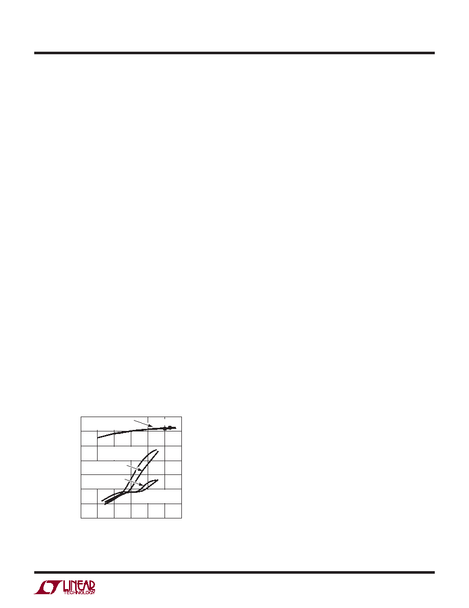
function begins to take effect at output signal levels
above 2VP-P and it becomes noticeable above 3.5VP-P.
This is illustrated in Figure 6; the LT6604-10 channel was
congured with unity passband gain and the input of the
lter was driven with a 1MHz signal. Because this voltage
limiting takes place well before the output stage of the
lter reaches the supply rails, the input/output behavior
of the IC shown in Figure 6 is relatively independent of
the power supply voltage.
The two ampliers inside the LT6604-10 channel have
independent control of their output common mode voltage
(see the Block Diagram section). The following guidelines
will optimize the performance of the lter.
VMID can be allowed to oat, but it must be bypassed to an
AC ground with a 0.01μF capacitor or some instability may
be observed. VMID can be driven from a low impedance
source, provided it remains at least 1.5V above V– and at
least 1.5V below V+. An internal resistor divider sets the
voltage of VMID. While the internal 11k resistors are well
matched, their absolute value can vary by ±20%. This
should be taken into consideration when connecting an
external resistor network to alter the voltage of VMID.
VOCM can be shorted to VMID for simplicity. If a different
common mode output voltage is required, connect VOCM
to a voltage source or resistor network. For 3V and 3.3V
supplies the voltage at VOCM must be less than or equal
to the mid supply level. For example, voltage (VOCM) ≤
1.65V on a single 3.3V supply. For power supply voltages
higher than 3.3V the voltage at VOCM can be set above mid
supply. The voltage on VOCM should not be more than 1V
below the voltage on VMID. The voltage on VOCM should
not be more than 2V above the voltage on VMID. VOCM is
a high impedance input.
The LT6604-10 was designed to process a variety of input
signals including signals centered on the mid-supply volt-
age and signals that swing between ground and a positive
voltage in a single supply system (Figure 1). The range of
allowable input common mode voltage (the average of VIN+
and VIN– in Figure 1) is determined by the power supply
level and gain setting (see “Electrical Characteristics”).
1MHz INPUT LEVEL (VP-P)
0
20
0
–20
–40
–60
–80
–100
–120
35
660410 F06
12
46
OUTPUT
LEVEL
(dBV)
3RD HARMONIC
85°C
1dB PASSBAND GAIN
COMPRESSION POINTS
1MHz 25°C
1MHz 85°C
3RD HARMONIC
25°C
2ND HARMONIC
25°C
2ND HARMONIC
85°C
Figure 6
相关PDF资料 |
PDF描述 |
|---|---|
| LM3702YDBP-220 | 1-CHANNEL POWER SUPPLY SUPPORT CKT, BGA9 |
| LTC2905IDDB8 | 2-CHANNEL POWER SUPPLY SUPPORT CKT, PDSO8 |
| LX1554ID-TR | 1 A SWITCHING CONTROLLER, 500 kHz SWITCHING FREQ-MAX, PDSO14 |
| L6230QTR | BRUSHLESS DC MOTOR CONTROLLER, 2.8 A, QCC32 |
| LM4040AIM-2.5 | 1-OUTPUT TWO TERM VOLTAGE REFERENCE, 2.5 V, PDSO8 |
相关代理商/技术参数 |
参数描述 |
|---|---|
| LTC6604IUFF-15-TRPBF | 制造商:LINER 制造商全称:Linear Technology 功能描述:Dual Very Low Noise, Differential Amplifi er and 15MHz Lowpass Filter |
| LTC6605-10 | 制造商:LINER 制造商全称:Linear Technology 功能描述:16-Bit, 20Msps Low Power ADC |
| LTC6605-14 | 制造商:LINER 制造商全称:Linear Technology 功能描述:16-Bit, 20Msps Low Power ADC |
| LTC6605-7 | 制造商:LINER 制造商全称:Linear Technology 功能描述:16-Bit, 20Msps Low Power Dual ADC |
| LTC6605CDJC-10#PBF | 功能描述:IC FILTER 10MHZ DUAL 22-DFN RoHS:是 类别:集成电路 (IC) >> 接口 - 滤波器 - 有源 系列:- 产品培训模块:Lead (SnPb) Finish for COTS Obsolescence Mitigation Program 标准包装:1,000 系列:- 滤波器类型:连续时间,带通低通 频率 - 截止或中心:150kHz 滤波器数:4 滤波器阶数:8th 电源电压:4.74 V ~ 11 V,±2.37 V ~ 5.5 V 安装类型:表面贴装 封装/外壳:28-SOIC(0.295",7.50mm 宽) 供应商设备封装:28-SOIC W 包装:带卷 (TR) |
发布紧急采购,3分钟左右您将得到回复。