- 您现在的位置:买卖IC网 > PDF目录149382 > LTC6604IUFF-10#TRPBF (LINEAR TECHNOLOGY CORP) SPECIALTY ANALOG CIRCUIT, PQCC34 PDF资料下载
参数资料
| 型号: | LTC6604IUFF-10#TRPBF |
| 厂商: | LINEAR TECHNOLOGY CORP |
| 元件分类: | 模拟信号调理 |
| 英文描述: | SPECIALTY ANALOG CIRCUIT, PQCC34 |
| 封装: | 4 X 7 MM, 0.75 MM HEIGHT, LEAD FREE, PLASTIC, QFN-34 |
| 文件页数: | 5/16页 |
| 文件大小: | 209K |
| 代理商: | LTC6604IUFF-10#TRPBF |
LT6604-10
13
660410fa
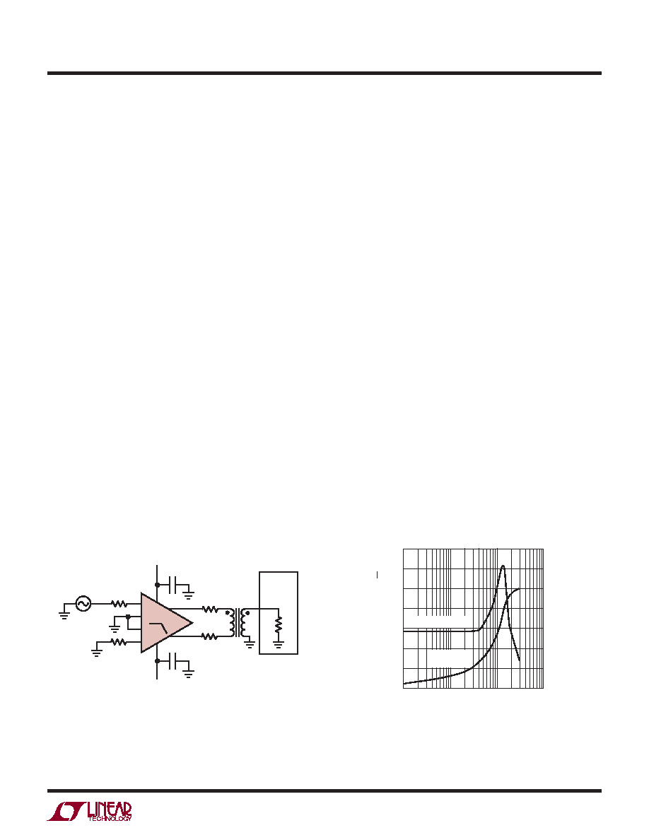
Figure 8 is plot of the noise spectral density as a function
of frequency for an LT6604-10 channel with RIN = 402Ω
using the xture of Figure 7 (the instrument noise has been
subtracted from the results). The noise at each output is
comprised of a differential component and a common
mode component. Using a transformer or combiner to
convert the differential outputs to single-ended signal
rejects the common mode noise and gives a true measure
of the S/N achievable in the system. Conversely, if each
output is measured individually and the noise power added
together, the resulting calculated noise level will be higher
than the true differential noise.
Power Dissipation
The LT6604-10 ampliers combine high speed with large
signal currents in a small package. There is a need to en-
sure that the die’s junction temperature does not exceed
150°C. The LT6604-10 has an Exposed Pad (pin 35) which
is connected to the lower supply (V–). Connecting the pad
to a ground plane helps to dissipate the heat generated
by the chip. Metal trace and plated through-holes can be
used to spread the heat generated by the device to the
backside of the PC board.
Junction temperature, TJ, is calculated from the ambient
temperature, TA, and power dissipation, PD. The power
dissipation is the product of supply voltage, VS, and
supply current, IS. Therefore, the junction temperature
is given by:
TJ = TA + (PD θJA) = TA + (VS IS θJA)
where the supply current, IS, is a function of signal level,
load impedance, temperature and common mode volt-
ages.
For a given supply voltage, the worst-case power dissipation
occurs when the differential input signal is maximum, the
common mode currents are maximum (see Applications
Information regarding Common Mode DC Currents), the
load impedance is small and the ambient temperature is
maximum. To compute the junction temperature, measure
the supply current under these worstcase conditions, use
34°C/W as the package thermal resistance, then apply the
equation for TJ. For example, using the circuit in Figure 3
with DC differential input voltage of 250mV, a differential
output voltage of 1V, no load resistance and an ambient
temperature of 85°C, the supply current (current into V+)
measures 48.9mA per channel. The resulting junction
temperature is: TJ = TA + (PD θJA) = 85 + (5 2 0.0489
34) = 102°C. The thermal resistance can be affected
by the amount of copper on the PCB that is connected to
V–. The thermal resistance of the circuit can increase if
the exposed pad is not connected to a large ground plane
with a number of vias.
APPLICATIONS INFORMATION
–
+
0.1μF
2.5V
–2.5V
–
+
25
27
4
34
6
2
29
7
RIN
25Ω
660410 F07
SPECTRUM
ANALYZER
INPUT
50Ω
VIN
COILCRAFT
TTWB-1010
1:1
1/2
LT6604-10
FREQUENCY (MHz)
0.1
SPECTRAL
DENSIT
Y
(nV
RMS
/√Hz)
INTEGRA
TED
NOISE
(μ
V
RMS
)
35
30
25
20
15
10
5
0
140
120
100
80
60
40
20
0
1.0
10
100
660410 F08
SPECTRAL DENSITY
INTEGRATED
NOISE
Figure 7
Figure 8
相关PDF资料 |
PDF描述 |
|---|---|
| LM3702YDBP-220 | 1-CHANNEL POWER SUPPLY SUPPORT CKT, BGA9 |
| LTC2905IDDB8 | 2-CHANNEL POWER SUPPLY SUPPORT CKT, PDSO8 |
| LX1554ID-TR | 1 A SWITCHING CONTROLLER, 500 kHz SWITCHING FREQ-MAX, PDSO14 |
| L6230QTR | BRUSHLESS DC MOTOR CONTROLLER, 2.8 A, QCC32 |
| LM4040AIM-2.5 | 1-OUTPUT TWO TERM VOLTAGE REFERENCE, 2.5 V, PDSO8 |
相关代理商/技术参数 |
参数描述 |
|---|---|
| LTC6604IUFF-15-TRPBF | 制造商:LINER 制造商全称:Linear Technology 功能描述:Dual Very Low Noise, Differential Amplifi er and 15MHz Lowpass Filter |
| LTC6605-10 | 制造商:LINER 制造商全称:Linear Technology 功能描述:16-Bit, 20Msps Low Power ADC |
| LTC6605-14 | 制造商:LINER 制造商全称:Linear Technology 功能描述:16-Bit, 20Msps Low Power ADC |
| LTC6605-7 | 制造商:LINER 制造商全称:Linear Technology 功能描述:16-Bit, 20Msps Low Power Dual ADC |
| LTC6605CDJC-10#PBF | 功能描述:IC FILTER 10MHZ DUAL 22-DFN RoHS:是 类别:集成电路 (IC) >> 接口 - 滤波器 - 有源 系列:- 产品培训模块:Lead (SnPb) Finish for COTS Obsolescence Mitigation Program 标准包装:1,000 系列:- 滤波器类型:连续时间,带通低通 频率 - 截止或中心:150kHz 滤波器数:4 滤波器阶数:8th 电源电压:4.74 V ~ 11 V,±2.37 V ~ 5.5 V 安装类型:表面贴装 封装/外壳:28-SOIC(0.295",7.50mm 宽) 供应商设备封装:28-SOIC W 包装:带卷 (TR) |
发布紧急采购,3分钟左右您将得到回复。