- 您现在的位置:买卖IC网 > PDF目录2156 > LTC6912CDE-1#TRPBF (Linear Technology)IC PGA DIGITAL R-R DUAL 12-DFN PDF资料下载
参数资料
| 型号: | LTC6912CDE-1#TRPBF |
| 厂商: | Linear Technology |
| 文件页数: | 10/24页 |
| 文件大小: | 0K |
| 描述: | IC PGA DIGITAL R-R DUAL 12-DFN |
| 标准包装: | 2,500 |
| 放大器类型: | 可编程增益 |
| 电路数: | 2 |
| 输出类型: | 满摆幅 |
| 转换速率: | 26 V/µs |
| 增益带宽积: | 33MHz |
| 电压 - 输入偏移: | 125µV |
| 电流 - 电源: | 2.25mA |
| 电流 - 输出 / 通道: | 35mA |
| 电压 - 电源,单路/双路(±): | 2.7 V ~ 10.5 V,±2.7 V ~ 5.25 V |
| 工作温度: | 0°C ~ 70°C |
| 安装类型: | 表面贴装 |
| 封装/外壳: | 12-WFDFN 裸露焊盘 |
| 供应商设备封装: | 12-DFN-EP(4x3) |
| 包装: | 带卷 (TR) |
LTC6912
18
6912fa
SHDN (GN-16 ONLY): CMOS Compatible Logic Hardware
Shutdown Input. The LTC6912-X has two shutdown modes.
One is a software shutdown state which can be software
programmed into either Channel A, Channel B, or both.
The software shutdown, when programmed to a particular
channel (state = 8), will disable that channel’s amplifier
and tri-state open its analog input and analog output. The
serial interface, however is still active. A hardware shut-
down occurs when the SHDN pin is pulled to the positive
rail. In this condition, both amplifiers and serial interface
are disabled. The SHDN pin is allowed to swing from V– to
10.5V above V–, regardless of V+ so long as the logic levels
meet the minimum requirements specified in the Electrical
Characteristics table. The SHDN pin is a high impedance
CMOS logic input, but has a small pull-down current
source (<10
A) which will force SHDN low if the logic
input is externally floated. On initial power up (with SHDN
open), or coming out of the hardware shutdown mode
(pulling SHDN to V–), both amplifiers are reset into the
power-on reset state (software shutdown mode, state = 8)
for both channels.
CS/LD: TTL/CMOS Compatible Logic Input. When this pin
is asserted low, the CLK pin is enabled, and the 8-bit shift
register serially shifts the shift register contents and
whatever data is present on the DIN pin into the shift
register on the rising edge of CLK. On the rising edge of
CS/LD, the contents of the shift register data are loaded
into the eight bit latch which configures the gain state of
both channel A and channel B amplifiers. A logic high on
CS/LD inhibits the CLK signal internally to the IC.
DIN: TTL/CMOS Compatible Logic Serial Data Input. The
serial interface is synchronously loaded MSB first via DIN
on the rising edge of CLK with CS/LD asserted low.
CLK: TTL/CMOS Compatible Logic Input. With CS/LD
asserted low, the clock synchronizes the loading of the
serial shift register on its rising and falling edges. Data is
shifted in at DIN on the rising edge of CLK and is shifted out
on DOUT on the falling edge of CLK.
DOUT: TTL/CMOS Compatible Logic Output. The MSB of
the shift register contents is shifted out at DOUT on the
falling edge of CLK. The output at DOUT swings between V+
and DGND, and is rated to drive approximately 15pF.
DGND: Digital Ground: The DGND pin defines the potential
from which LOGIC levels VIH and VIL for the 3-wire serial
digital interface are referenced. The recommended con-
nection of DGND depends on how power is applied to the
LTC6912 (See Figures 2, 3, and 4). (CAVEAT: Under no
conditions is DGND to exceed either supply pins V+ and
V–, which could result in damage to the IC if not current
limited.)
Single power supply applications typically use V– for the
system signal ground. The preferred connection for DGND
is therefore V– (See Figure 2).
Dual supply applications with symmetrical supplies (such
as
±5V) have a natural system ground potential of zero
volts, in which the DGND pin can be tied to, making the
zero volt ground plane the logic reference (Figure 3).
Finally, if dual asymmetrical power supplies are used, the
system ground is still the natural ground plane voltage.
V–, V+: Power Supply Pins. The V+ and V– pins should be
bypassed with 0.1
F capacitors to an adequate analog
ground plane using the shortest possible wiring. Electri-
cally clean supplies and a low impedance ground are
important for the high dynamic range available from the
LTC6912 (see further details under the AGND pin descrip-
tion). Low noise linear power supplies are recommended.
Switching power supplies require special care to prevent
switching noise coupling into the signal path, reducing
dynamic range.
UU
U
PI FU CTIO S
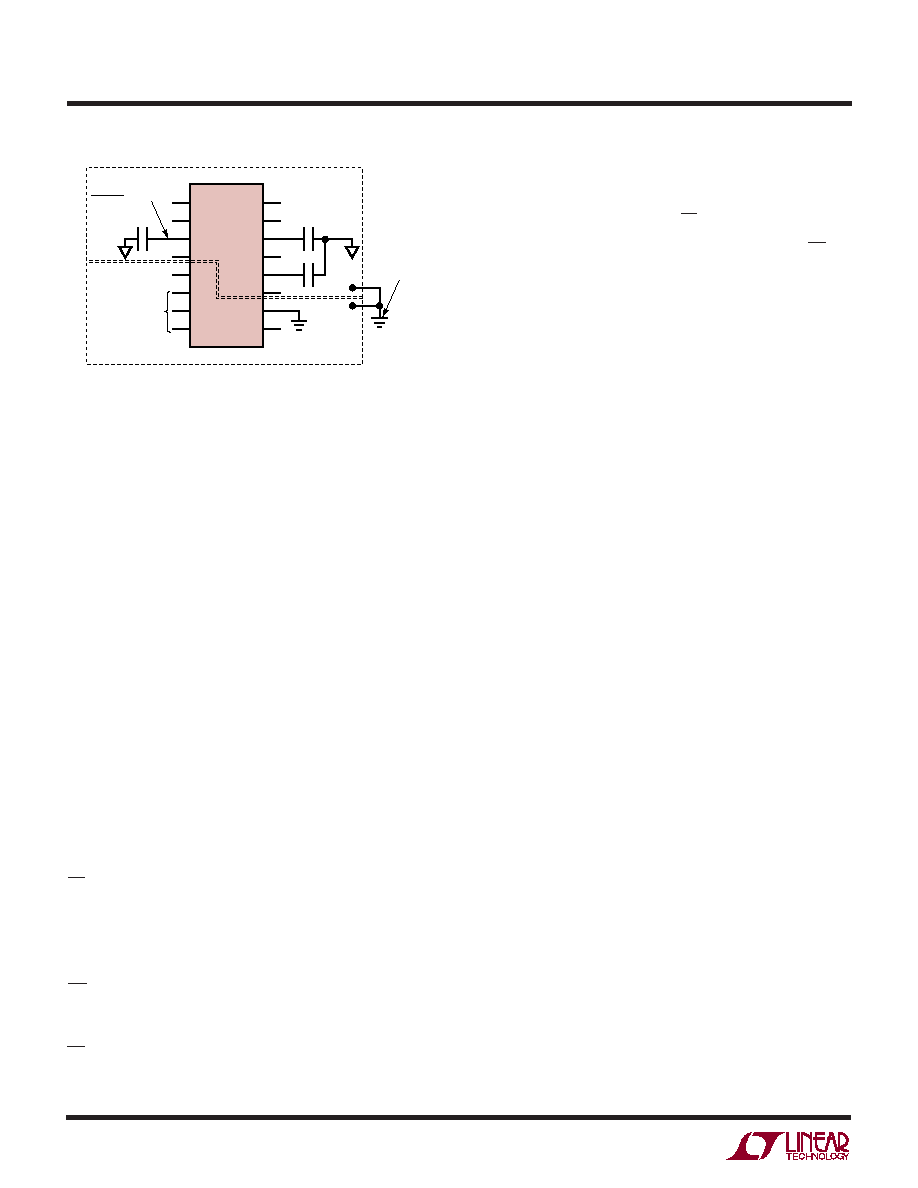
Figure 4. Asymmetrical Dual Supply Ground Plane Connection
1
2
3
4
5
6
7
8
16
15
14
13
12
11
10
9
LTC6912-X
SERIAL
INTERFACE
0.1
F
0.1
F
V+
V–
DIGITAL GROUND PLANE
ANALOG GROUND PLANE
≥0.1F
V+ + V–
2
REFERENCE
6912 F04
SINGLE-POINT
SYSTEM GND
相关PDF资料 |
PDF描述 |
|---|---|
| LTC6915IGN#TRPBF | IC PGA DIGITAL PREC 0DRFT 16SSOP |
| M3CA0207 | MIC HOLDER WM-52B/54B/55A D/56A |
| MA-302-55E | HEATSINK FOR TO-247 TO-264 |
| MA2062-HVL.GN | FN 220/240VAC 60X25MM 17.5/18CFM |
| MA2072-HVL.GN | FAN 220/240VAC 70X25MM 28/29CFM |
相关代理商/技术参数 |
参数描述 |
|---|---|
| LTC6912CDE-2 | 制造商:LINER 制造商全称:Linear Technology 功能描述:Dual Programmable Gain Amplifiers with Serial Digital Interface |
| LTC6912CDE-2#PBF | 功能描述:IC PGA DIGITAL R-R DUAL 12-DFN RoHS:是 类别:集成电路 (IC) >> Linear - Amplifiers - Instrumentation 系列:- 其它有关文件:Automotive Product Guide 产品培训模块:Lead (SnPb) Finish for COTS Obsolescence Mitigation Program 标准包装:1 系列:- 放大器类型:通用 电路数:1 输出类型:满摆幅 转换速率:3 V/µs 增益带宽积:10MHz -3db带宽:- 电流 - 输入偏压:1pA 电压 - 输入偏移:70µV 电流 - 电源:2.5mA 电流 - 输出 / 通道:48mA 电压 - 电源,单路/双路(±):2.7 V ~ 5.5 V,±1.35 V ~ 2.75 V 工作温度:-40°C ~ 125°C 安装类型:表面贴装 封装/外壳:SOT-23-6 供应商设备封装:SOT-6 包装:Digi-Reel® 其它名称:MAX4475AUT#TG16DKR |
| LTC6912CDE-2#TRPBF | 功能描述:IC PGA DIGITAL R-R DUAL 12-DFN RoHS:是 类别:集成电路 (IC) >> Linear - Amplifiers - Instrumentation 系列:- 其它有关文件:Automotive Product Guide 产品培训模块:Lead (SnPb) Finish for COTS Obsolescence Mitigation Program 标准包装:1 系列:- 放大器类型:通用 电路数:1 输出类型:满摆幅 转换速率:3 V/µs 增益带宽积:10MHz -3db带宽:- 电流 - 输入偏压:1pA 电压 - 输入偏移:70µV 电流 - 电源:2.5mA 电流 - 输出 / 通道:48mA 电压 - 电源,单路/双路(±):2.7 V ~ 5.5 V,±1.35 V ~ 2.75 V 工作温度:-40°C ~ 125°C 安装类型:表面贴装 封装/外壳:SOT-23-6 供应商设备封装:SOT-6 包装:Digi-Reel® 其它名称:MAX4475AUT#TG16DKR |
| LTC6912CGN-1 | 制造商:Linear Technology 功能描述:SP Amp Variable Gain Amp Dual R-R I/O ±5.25V/10.5V 16-Pin SSOP N |
| LTC6912CGN-1#PBF | 功能描述:IC PGA DIGITAL R-R DUAL 16SSOP RoHS:是 类别:集成电路 (IC) >> Linear - Amplifiers - Instrumentation 系列:- 标准包装:50 系列:LinCMOS™ 放大器类型:通用 电路数:4 输出类型:- 转换速率:0.05 V/µs 增益带宽积:110kHz -3db带宽:- 电流 - 输入偏压:0.7pA 电压 - 输入偏移:210µV 电流 - 电源:57µA 电流 - 输出 / 通道:30mA 电压 - 电源,单路/双路(±):3 V ~ 16 V,±1.5 V ~ 8 V 工作温度:-40°C ~ 85°C 安装类型:表面贴装 封装/外壳:14-SOIC(0.154",3.90mm 宽) 供应商设备封装:14-SOIC 包装:管件 产品目录页面:865 (CN2011-ZH PDF) 其它名称:296-1834296-1834-5 |
发布紧急采购,3分钟左右您将得到回复。