- 您现在的位置:买卖IC网 > PDF目录2156 > LTC6912CDE-1#TRPBF (Linear Technology)IC PGA DIGITAL R-R DUAL 12-DFN PDF资料下载
参数资料
| 型号: | LTC6912CDE-1#TRPBF |
| 厂商: | Linear Technology |
| 文件页数: | 11/24页 |
| 文件大小: | 0K |
| 描述: | IC PGA DIGITAL R-R DUAL 12-DFN |
| 标准包装: | 2,500 |
| 放大器类型: | 可编程增益 |
| 电路数: | 2 |
| 输出类型: | 满摆幅 |
| 转换速率: | 26 V/µs |
| 增益带宽积: | 33MHz |
| 电压 - 输入偏移: | 125µV |
| 电流 - 电源: | 2.25mA |
| 电流 - 输出 / 通道: | 35mA |
| 电压 - 电源,单路/双路(±): | 2.7 V ~ 10.5 V,±2.7 V ~ 5.25 V |
| 工作温度: | 0°C ~ 70°C |
| 安装类型: | 表面贴装 |
| 封装/外壳: | 12-WFDFN 裸露焊盘 |
| 供应商设备封装: | 12-DFN-EP(4x3) |
| 包装: | 带卷 (TR) |
LTC6912
19
6912fa
UU
U
PI FU CTIO S
APPLICATIO S I FOR ATIO
WU
U
Functional Description
The LTC6912-X is a small outline, wideband, inverting
two-channel amplifier with voltage gains that are indepen-
dently programmable. Each delivers a choice of eight
voltage gains, configurable through a 3-wire serial digital
interface, which accepts TTL or CMOS logic levels (See
Figure 5). Tables 1 and 2 list the nominal gains for the
LTC6912-1 and LTC6912-2 respectively. Gain control
within the amplifier occurs by switching resistors from a
matched array in or out of a closed-loop op amp circuit
using MOS analog switches (Figure 1). The bandwidths of
the individual amplifiers depend on gain setting. The
Typical Performance Characteristics section shows mea-
sured frequency responses.
Description of the 3-Wire SPI Interface
Gain control of each amplifier is independently program-
mable using the 3-wire SPI interface (see Figure 5). Logic
levels for the LTC6912 3-wire serial interface are TTL/
CMOS compatible. When CS/LD is low, the serial data on
DIN is shifted into an 8-bit shift-register on the rising edge
of the clock, with the MSB transferred first. Serial data on
DOUT is shifted out on the clock’s falling edge. A rising edge
on CS/LD will latch the shift-register’s contents into an 8-
bit D-latch and disable the clock internally on the IC. The
upper nibble of the D-latch (4 most significant bits),
configure the gain for the B-channel amplifier. The lower
nibble of the D-latch (4 least significant bits), configures
the gain for the A-channel amplifier. Tables 1 and 2 detail
the nominal gains and respective gain codes. Care must be
taken to ensure CLK is taken low before CS/LD is pulled
low to avoid an extra internal clock pulse to the input of the
8-bit shift-register (See Figure 5).
DOUT is active in all states, therefore DOUT cannot be
“wire-OR’d” to other SPI outputs.
An LTC6912 may be daisy-chained with other LTC6912s
or other devices having serial interfaces by connecting the
DOUT to the DIN of the next chip while CLK and CS/LD
remain common to all chips in the daisy chain. The serial
data is clocked to all the chips then the CS/LD signal is
pulled high to update all of them simultaneously. Figure 6
shows an example of two LTC6912s in a daisy chained SPI
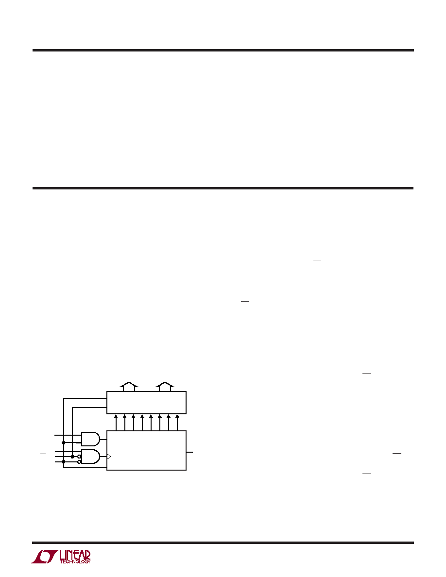
Figure 5. Serial Digital Interface Block Diagram
CLK
CS/LD
SHDN
6912 F05
LOWER NIBBLE UPPER NIBBLE
8-BIT LATCH
8-BIT
SHIFT-REGISTER
CHANNEL A
CHANNEL B
Q0 Q1 Q2 Q3 Q4 Q5 Q6 Q7
DOUT
LSB
MSB
RESET
LE
DIN
OUT A, OUT B: Analog Output. These pins are the output
of the A and B channel amplifiers respectively. Each
operational amplifier can swing rail-to-rail (V+ to V–) as
specified in the Electrical Characteristics table. For best
performance, loading the output as lightly as possible will
minimize signal distortion and gain error. The Electrical
Characteristics table shows performance at output cur-
rents up to 10mA, and the current limits which occur when
the output is shorted midsupply at 2.7V and
±5V supplies.
Output current above 10mA is possible but current-limit-
ing circuitry will begin to affect amplifier performance at
approximately 20mA. Long-term operation above 20mA
output is not recommended. Do not exceed maximum
junction temperature of 150
°C for a GN and 125°C for a
DFN package. The output will drive capacitive loads up to
50pF. Capacitances higher than 50pF should be isolated
by a series resistor (10
or higher).
相关PDF资料 |
PDF描述 |
|---|---|
| LTC6915IGN#TRPBF | IC PGA DIGITAL PREC 0DRFT 16SSOP |
| M3CA0207 | MIC HOLDER WM-52B/54B/55A D/56A |
| MA-302-55E | HEATSINK FOR TO-247 TO-264 |
| MA2062-HVL.GN | FN 220/240VAC 60X25MM 17.5/18CFM |
| MA2072-HVL.GN | FAN 220/240VAC 70X25MM 28/29CFM |
相关代理商/技术参数 |
参数描述 |
|---|---|
| LTC6912CDE-2 | 制造商:LINER 制造商全称:Linear Technology 功能描述:Dual Programmable Gain Amplifiers with Serial Digital Interface |
| LTC6912CDE-2#PBF | 功能描述:IC PGA DIGITAL R-R DUAL 12-DFN RoHS:是 类别:集成电路 (IC) >> Linear - Amplifiers - Instrumentation 系列:- 其它有关文件:Automotive Product Guide 产品培训模块:Lead (SnPb) Finish for COTS Obsolescence Mitigation Program 标准包装:1 系列:- 放大器类型:通用 电路数:1 输出类型:满摆幅 转换速率:3 V/µs 增益带宽积:10MHz -3db带宽:- 电流 - 输入偏压:1pA 电压 - 输入偏移:70µV 电流 - 电源:2.5mA 电流 - 输出 / 通道:48mA 电压 - 电源,单路/双路(±):2.7 V ~ 5.5 V,±1.35 V ~ 2.75 V 工作温度:-40°C ~ 125°C 安装类型:表面贴装 封装/外壳:SOT-23-6 供应商设备封装:SOT-6 包装:Digi-Reel® 其它名称:MAX4475AUT#TG16DKR |
| LTC6912CDE-2#TRPBF | 功能描述:IC PGA DIGITAL R-R DUAL 12-DFN RoHS:是 类别:集成电路 (IC) >> Linear - Amplifiers - Instrumentation 系列:- 其它有关文件:Automotive Product Guide 产品培训模块:Lead (SnPb) Finish for COTS Obsolescence Mitigation Program 标准包装:1 系列:- 放大器类型:通用 电路数:1 输出类型:满摆幅 转换速率:3 V/µs 增益带宽积:10MHz -3db带宽:- 电流 - 输入偏压:1pA 电压 - 输入偏移:70µV 电流 - 电源:2.5mA 电流 - 输出 / 通道:48mA 电压 - 电源,单路/双路(±):2.7 V ~ 5.5 V,±1.35 V ~ 2.75 V 工作温度:-40°C ~ 125°C 安装类型:表面贴装 封装/外壳:SOT-23-6 供应商设备封装:SOT-6 包装:Digi-Reel® 其它名称:MAX4475AUT#TG16DKR |
| LTC6912CGN-1 | 制造商:Linear Technology 功能描述:SP Amp Variable Gain Amp Dual R-R I/O ±5.25V/10.5V 16-Pin SSOP N |
| LTC6912CGN-1#PBF | 功能描述:IC PGA DIGITAL R-R DUAL 16SSOP RoHS:是 类别:集成电路 (IC) >> Linear - Amplifiers - Instrumentation 系列:- 标准包装:50 系列:LinCMOS™ 放大器类型:通用 电路数:4 输出类型:- 转换速率:0.05 V/µs 增益带宽积:110kHz -3db带宽:- 电流 - 输入偏压:0.7pA 电压 - 输入偏移:210µV 电流 - 电源:57µA 电流 - 输出 / 通道:30mA 电压 - 电源,单路/双路(±):3 V ~ 16 V,±1.5 V ~ 8 V 工作温度:-40°C ~ 85°C 安装类型:表面贴装 封装/外壳:14-SOIC(0.154",3.90mm 宽) 供应商设备封装:14-SOIC 包装:管件 产品目录页面:865 (CN2011-ZH PDF) 其它名称:296-1834296-1834-5 |
发布紧急采购,3分钟左右您将得到回复。