- 您现在的位置:买卖IC网 > PDF目录16318 > LTC694CS8#PBF (Linear Technology)IC MPU SUPERVISORY CIRCUIT 8SOIC PDF资料下载
参数资料
| 型号: | LTC694CS8#PBF |
| 厂商: | Linear Technology |
| 文件页数: | 11/20页 |
| 文件大小: | 0K |
| 描述: | IC MPU SUPERVISORY CIRCUIT 8SOIC |
| 标准包装: | 100 |
| 类型: | 简单复位/加电复位 |
| 监视电压数目: | 1 |
| 输出: | 开路漏极或开路集电极 |
| 复位: | 高有效/低有效 |
| 复位超时: | 最小为 140 ms |
| 电压 - 阀值: | 4.65V |
| 工作温度: | 0°C ~ 70°C |
| 安装类型: | 表面贴装 |
| 封装/外壳: | 8-SOIC(0.154",3.90mm 宽) |
| 供应商设备封装: | 8-SOIC |
| 包装: | 管件 |
| 产品目录页面: | 1336 (CN2011-ZH PDF) |
�� �
�
�LTC690/LTC691�
�LTC694/LTC695�
�APPLICATIONS� INFORMATION�
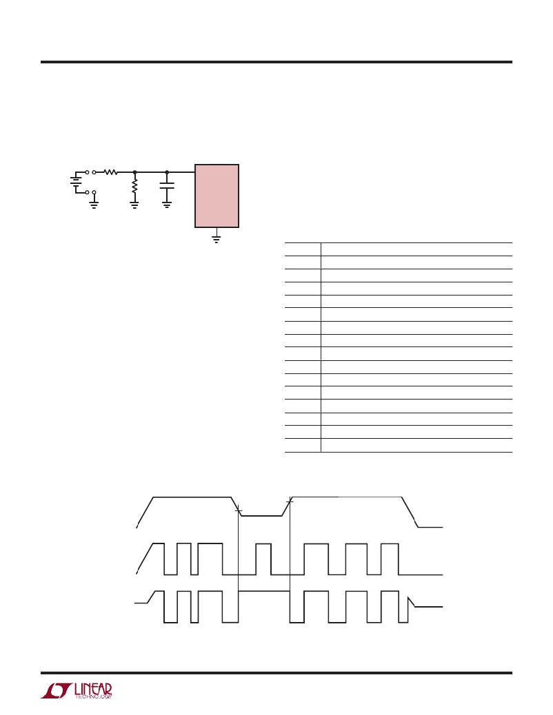
�If� battery� connections� are� made� through� long� wires,� a�
�10Ω� to� 100Ω� series� resistor� and� a� 0.1μF� capacitor� are�
�recommended� to� prevent� any� overshoot� beyond� V� CC� due�
�to� the� lead� inductance� (Figure� 4).�
�input� of� battery-backed� up� CMOS� RAM.� CE� OUT� can� also�
�be� used� to� drive� the� Store� or� Write� input� of� an� EEPROM,�
�EAROM� or� NOVRAM� to� achieve� similar� protection.� Figure�
�5� shows� the� timing� diagram� of� CE� IN� and� CE� OUT.�
�10�
�4.3M�
�0.1μF�
�V� BATT�
�LTC690�
�LTC691�
�LTC694�
�LTC695�
�GND�
�CE� IN� can� be� derived� from� the� microprocessor’s� address�
�decoder� output.� Figure� 6� shows� a� typical� nonvolatile� CMOS�
�RAM� application.�
�Memory� protection� can� also� be� achieved� with� the� LTC690�
�and� LTC694� by� using� RESET� as� shown� in� Figure� 7.�
�690� F04�
�Table� 1.� Input� and� Output� Status� in� Battery� Back-Up� Mode�
�Figure� 4.� 10Ω/0.1μF� Combination� Eliminates� Inductive�
�Overshoot� and� Prevents� Spurious� Resets� During� Battery�
�Replacement�
�Table� 1� shows� the� state� of� each� pin� during� battery� back-up.�
�When� the� battery� switchover� section� is� not� used,� connect�
�V� BATT� to� GND� and� V� OUT� to� V� CC� .�
�SIGNAL�
�V� CC�
�V� OUT�
�V� BATT�
�BATT� ON�
�PFI�
�PFO�
�STATUS�
�C2� monitors� V� CC� for� active� switchover.�
�V� OUT� is connected to V� BATT� through an internal PMOS switch.�
�The� supply� current� is� 1μA� maximum.�
�Logic high. The open-circuit output voltage is equal to V� OUT� .�
�Power� failure� input� is� ignored.�
�Logic� low�
�Memory� Protection�
�The� LTC691� and� LTC695� include� memory� protection� cir-�
�cuitry� that� ensures� the� integrity� of� the� data� in� memory� by�
�preventing� write� operations� when� V� CC� is� at� invalid� level.�
�Two� additional� pins,� CE� IN� and� CE� OUT,� control� the� Chip�
�Enable� or� Write� inputs� of� CMOS� RAM.� When� V� CC� is� 5V,�
�CE� OUT� follows� CE� IN� with� a� typical� propagation� delay� of�
�20ns.� When� V� CC� falls� below� the� reset� voltage� threshold� or�
�V� BATT� ,� CE� OUT� is� forced� high,� independent� of� CE� IN.� CE�
�OUT� is� an� alternative� signal� to� drive� the� CE� ,� CS� ,� or� Write�
�RESET� Logic� low�
�RESET� Logic high. The open-circuit output voltage is equal to V� OUT� .�
�LOW?LINE� Logic� low�
�WDI� Watchdog� input� is� ignored.�
�WDO� Logic high. The open-circuit output voltage is equal to V� OUT� .�
�CE� IN� Chip?Enable� Input� is� ignored.�
�CE� OUT� Logic high. The open-circuit output voltage is equal to V� OUT� .�
�OSC� IN� OSC� IN� is� ignored.�
�OSC� SEL� OSC� SEL� is� ignored.�
�V� CC�
�V1�
�V2�
�V1� =� RESET� VOLTAGE� THRESHOLD�
�V2� =� RESET� VOLTAGE� THRESHOLD� +�
�RESET� THRESHOLD� HYSTERESIS�
�CE� IN�
�CE� OUT�
�V� OUT� =� V� BATT�
�Figure� 5.� Timing� Diagram� for� CE� IN� and� CE� OUT�
�V� OUT� =� V� BATT�
�690� F05�
�690ff�
�For� more� information� www.linear.com/690�
�11�
�相关PDF资料 |
PDF描述 |
|---|---|
| A3DDH-4018G | IDC CABLE - AKR40H/AE40G/AKR40H |
| GEC25DRTI-S93 | CONN EDGECARD 50POS DIP .100 SLD |
| GEC44DRXS | CONN EDGECARD 88POS DIP .100 SLD |
| A3BKB-2018M | IDC CABLE- ASR20B/AE20M/APK20B |
| GBC22DRTH-S93 | CONN EDGECARD 44POS DIP .100 SLD |
相关代理商/技术参数 |
参数描述 |
|---|---|
| LTC694I | 制造商:LINER 制造商全称:Linear Technology 功能描述:Microprocessor Supervisory Circuits |
| LTC694I-3.3 | 制造商:LINER 制造商全称:Linear Technology 功能描述:3.3V Microprocessor Supervisory Circuits |
| LTC694IN-3.3 | 制造商:未知厂家 制造商全称:未知厂家 功能描述:Power Supply Supervisor |
| LTC694IN8 | 功能描述:IC MPU SUPERVISORY CIRCUIT 8-DIP RoHS:否 类别:集成电路 (IC) >> PMIC - 监控器 系列:- 标准包装:1 系列:- 类型:简单复位/加电复位 监视电压数目:1 输出:开路漏极或开路集电极 复位:高有效 复位超时:- 电压 - 阀值:1.8V 工作温度:-40°C ~ 125°C 安装类型:表面贴装 封装/外壳:6-TSOP(0.059",1.50mm 宽)5 引线 供应商设备封装:5-TSOP 包装:剪切带 (CT) 其它名称:NCP301HSN18T1GOSCT |
| LTC694IN8#PBF | 功能描述:IC MPU SUPERVISORY CIRCUIT 8-DIP RoHS:是 类别:集成电路 (IC) >> PMIC - 监控器 系列:- 标准包装:1 系列:- 类型:简单复位/加电复位 监视电压数目:1 输出:开路漏极或开路集电极 复位:高有效 复位超时:- 电压 - 阀值:1.8V 工作温度:-40°C ~ 125°C 安装类型:表面贴装 封装/外壳:6-TSOP(0.059",1.50mm 宽)5 引线 供应商设备封装:5-TSOP 包装:剪切带 (CT) 其它名称:NCP301HSN18T1GOSCT |
发布紧急采购,3分钟左右您将得到回复。