- 您现在的位置:买卖IC网 > PDF目录80093 > LTC695IN-3.3#TRPBF (LINEAR TECHNOLOGY CORP) 1-CHANNEL POWER SUPPLY MANAGEMENT CKT, PDIP16 PDF资料下载
参数资料
| 型号: | LTC695IN-3.3#TRPBF |
| 厂商: | LINEAR TECHNOLOGY CORP |
| 元件分类: | 电源管理 |
| 英文描述: | 1-CHANNEL POWER SUPPLY MANAGEMENT CKT, PDIP16 |
| 封装: | 0.300 INCH, LEAD FREE, PLASTIC, DIP-16 |
| 文件页数: | 4/20页 |
| 文件大小: | 189K |
| 代理商: | LTC695IN-3.3#TRPBF |
LTC694-3.3/LTC695-3.3
12
69453fb
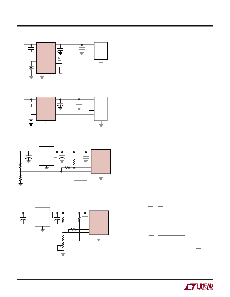
CE IN can be derived from the microprocessor’s address
decoder output. Figure 6 shows a typical nonvolatile CMOS
RAM application.
Memory protection can also be achieved with the LTC694-
3.3 by using RESET as shown in Figure 7.
Power-Fail Warning
The LTC694-3.3/LTC695-3.3 generate a Power Failure Out-
put (PFO) for early warning of failure in the microprocessor’s
power supply. This is accomplished by comparing the
power failure input (PFI) with an internal 1.3V reference.
PFO goes low when the voltage at the PFI pin is less than
1.3V. Typically PFI is driven by an external voltage divider
(R1 and R2 in Figures 8 and 9) which senses either an
unregulated DC input or a regulated 3.3V output. The
voltage divider ratio can be chosen such that the voltage
at the PFI pin falls below 1.3V several milliseconds before
the 3.3V supply falls below the maximum reset voltage
threshold 3.0V. PFO is normally used to interrupt the
microprocessor to execute shutdown procedure between
PFO and RESET or RESET.
The power-fail comparator, C3, does not have hysteresis.
Hysteresis can be added however, by connecting a resistor
between the PFO output and the noninverting PFI input
pin as shown in Figures 8 and 9. The upper and lower trip
points in the comparator are established as follows:
When PFO output is low, R3 sinks current from the sum-
ming junction at the PFI pin.
VH =1.3V 1+
R1
R2
+
R1
R3
When PFO output is high, the series combination of R3
and R4 source current into the PFI summing junction.
VL =1.3V 1+
R1
R2
–
(3.3V ±1.3V)R1
1.3V(R3
+R4)
Assuming R4 << R3, VHYSTERESIS = 3.3V
R1
R3
APPLICATIONS INFORMATION
Figure 6. A Typical Nonvolatile CMOS RAM Application
3.3V
2.4V
0.1μF
10μF
VBATT
VCC
LTC695-3.3
VOUT
GND
694/5-3.3 F06
VCC
RESET
CE IN
CE OUT
RESET
0.1μF
TO μP
FROM DECODER
CS
30ns PROPAGATION DELAY
62512
RAM
GND
+
3.3V
2.4V
0.1μF
10μF
VBATT
VCC
VOUT
GND
694/5-3.3 F07
VCC
RESET
0.1μF
CS
62128
RAM
CS1
CS2
GND
LTC694-3.3
+
Figure 7. Write Protect for RAM with LTC694-3.3
100μF
694/5-3.3 F08
VCC
0.1μF
10μF
TO μP
PFO
GND
VIN ≥ 5V
R4
10k
PFI
LTC694-3.3
LTC695-3.3
R1
51k
R2
16k
R3
200k
3.3V
VIN
VOUT
LT1129-3.3
SHDN
OUT SENSE
ADJ
+
Figure 8. Monitoring
Unregulated DC Supply with the
LTC694-3.3/LTC695-3.3’s Power-Fail Comparator
Figure 9. Monitoring
Regulated DC Supply with the
LTC694-3.3/LTC695-3.3’s Power-Fail Comparator
10μF
694/5-3.3 F09
0.1μF
TO μP
VIN 6.5V
10μF
R3
2.7M
3.3V
R1
27k
R2
16k
R5
5k
VCC
GND
PFO
PFI
LTC694-3.3
LTC695-3.3
R4
10k
VIN
VOUT
LT1129-3.3
SHDN
OUT SENSE
ADJ
+
相关PDF资料 |
PDF描述 |
|---|---|
| L6725A | 20 A SWITCHING CONTROLLER, 500 kHz SWITCHING FREQ-MAX, PDSO16 |
| LV8052GP | STEPPER MOTOR CONTROLLER, 0.6 A, QCC24 |
| LK1301-9EPD5T | 1-OUTPUT 150 W AC-DC REG PWR SUPPLY MODULE |
| LK1501-9EPDDTB1 | 1-OUTPUT 150 W AC-DC REG PWR SUPPLY MODULE |
| LK1601-9ERD0T | 1-OUTPUT 150 W AC-DC REG PWR SUPPLY MODULE |
相关代理商/技术参数 |
参数描述 |
|---|---|
| LTC695INPBF | 制造商:LINER 制造商全称:Linear Technology 功能描述:Microprocessor Supervisory Circuits |
| LTC695IN-PBF | 制造商:LINER 制造商全称:Linear Technology 功能描述:Microprocessor Supervisory Circuits |
| LTC695IS | 制造商:未知厂家 制造商全称:未知厂家 功能描述:Power Supply Supervisor |
| LTC695IS-3.3 | 制造商:未知厂家 制造商全称:未知厂家 功能描述:Power Supply Supervisor |
| LTC695ISW | 功能描述:IC MPU SUPERVISRY CIRCUIT 16SOIC RoHS:否 类别:集成电路 (IC) >> PMIC - 监控器 系列:- 标准包装:1 系列:- 类型:简单复位/加电复位 监视电压数目:1 输出:开路漏极或开路集电极 复位:高有效 复位超时:- 电压 - 阀值:1.8V 工作温度:-40°C ~ 125°C 安装类型:表面贴装 封装/外壳:6-TSOP(0.059",1.50mm 宽)5 引线 供应商设备封装:5-TSOP 包装:剪切带 (CT) 其它名称:NCP301HSN18T1GOSCT |
发布紧急采购,3分钟左右您将得到回复。