参数资料
| 型号: | LTC6991CDCB#TRMPBF |
| 厂商: | Linear Technology |
| 文件页数: | 19/24页 |
| 文件大小: | 0K |
| 描述: | IC OSC SILICON 977HZ 6-DFN |
| 产品培训模块: | TimerBlox Family Timing Devices |
| 产品目录绘图: | LTC699_DFN |
| 特色产品: | LTC?6991 Silicon Oscillator TimerBlox? |
| 标准包装: | 1 |
| 系列: | TimerBlox® |
| 类型: | 振荡器 - 硅 |
| 频率: | 29.1µHz ~ 977Hz |
| 电源电压: | 2.25 V ~ 5.5 V |
| 电流 - 电源: | 135µA |
| 工作温度: | 0°C ~ 70°C |
| 封装/外壳: | 6-WFDFN 裸露焊盘 |
| 包装: | 标准包装 |
| 供应商设备封装: | 6-DFN-EP(2x3) |
| 安装类型: | 表面贴装 |
| 配用: | DC1562A-B-ND - BOARD EVAL LTC6991 |
| 其它名称: | LTC6991CDCB#TRMPBFDKR |
LTC6991
4
6991fb
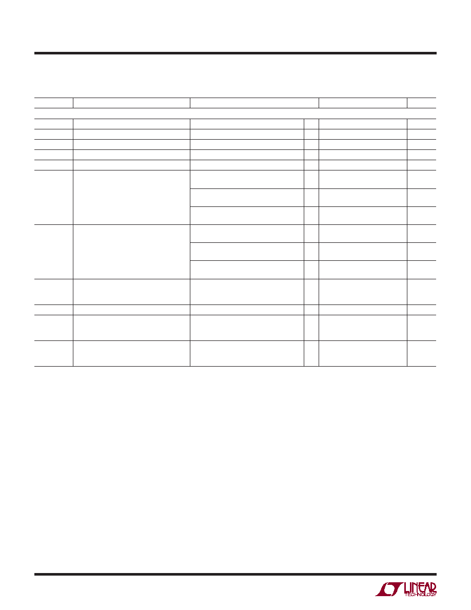
ELECTRICAL CHARACTERISTICS The l denotes the specifications which apply over the full operating
temperature range, otherwise specifications are at TA = 25°C. Test conditions are V+ = 2.25V to 5.5V, RST = 0V, DIVCODE = 0 to 15
(NDIV = 1 to 221), RSET = 50k to 800k, RLOAD = ∞, CLOAD = 5pF unless otherwise noted.
SYMBOL
PARAMETER
CONDITIONS
MIN
TYP
MAX
UNITS
Digital I/O
RST Pin Input Capacitance
2.5
pF
RST Pin Input Current
RST = 0V to V+
±10
nA
VIH
High Level RST Pin Input Voltage
(Note 6)
l
0.7 V+
V
VIL
Low Level RST Pin Input Voltage
(Note 6)
l
0.3 V+
V
IOUT(MAX)
Output Output Current
V+ = 2.7V to 5.5V
±20
mA
VOH
High Level Output Voltage (Note 7)
V+ = 5.5V
IOUT = –1mA
IOUT = –16mA
l
5.45
4.84
5.48
5.15
V
V+ = 3.3V
IOUT = –1mA
IOUT = –10mA
l
3.24
2.75
3.27
2.99
V
V+ = 2.25V
IOUT = –1mA
IOUT = –8mA
l
2.17
1.58
2.21
1.88
V
VOL
Low Level Output Voltage (Note 7)
V+ = 5.5V
IOUT = 1mA
IOUT = 16mA
l
0.02
0.26
0.04
0.54
V
V+ = 3.3V
IOUT = 1mA
IOUT = 10mA
l
0.03
0.22
0.05
0.46
V
V+ = 2.25V
IOUT = 1mA
IOUT = 8mA
l
0.03
0.26
0.07
0.54
V
tRST
Reset Propagation Delay
V+ = 5.5V
V+ = 3.3V
V+ = 2.25V
16
24
40
ns
tWIDTH
Minimum Input Pulse Width
V+ = 3.3V
5
ns
tr
Output Rise Time (Note 8)
V+ = 5.5V
V+ = 3.3V
V+ = 2.25V
1.1
1.7
2.7
ns
tf
Output Fall Time (Note 8)
V+ = 5.5V
V+ = 3.3V
V+ = 2.25V
1.0
1.6
2.4
ns
Note 1: Stresses beyond those listed under Absolute Maximum Ratings
may cause permanent damage to the device. Exposure to any Absolute
Maximum Rating condition for extended periods may affect device
reliability and lifetime.
Note 2: The LTC6991C is guaranteed functional over the operating
temperature range of –40°C to 85°C.
Note 3: The LTC6991C is guaranteed to meet specified performance from
0°C to 70°C. The LTC6991C is designed, characterized and expected to
meet specified performance from –40°C to 85°C but it is not tested or
QA sampled at these temperatures. The LTC6991I is guaranteed to meet
specified performance from –40°C to 85°C. The LTC6991H is guaranteed
to meet specified performance from –40°C to 125°C. The LTC6991MP is
guaranteed to meet specified performance from –55°C to 125°C.
Note 4: Frequency accuracy is defined as the deviation from the fOUT
equation, assuming RSET is used to program the frequency.
Note 5: See Operation section, Table 1 and Figure 2 for a full explanation
of how the DIV pin voltage selects the value of DIVCODE.
Note 6: The RST pin has hysteresis to accommodate slow rising or falling
signals. The threshold voltages are proportional to V+. Typical values can
be estimated at any supply voltage using VRST(RISING) ≈ 0.55 V+ + 185mV
and VRST(FALLING) ≈ 0.48 V+ – 155mV.
Note 7: To conform to the Logic IC Standard, current out of a pin is
arbitrarily given a negative value.
Note 8: Output rise and fall times are measured between the 10% and the
90% power supply levels with 5pF output load. These specifications are
based on characterization.
Note 9: Settling time is the amount of time required for the output to settle
within ±1% of the final frequency after a 0.5× or 2× change in ISET.
Note 10: Jitter is the ratio of the deviation of the period to the mean of the
period. This specification is based on characterization and is not 100%
tested.
Note 11: Long-term drift of silicon oscillators is primarily due to the
movement of ions and impurities within the silicon and is tested at 30°C
under otherwise nominal operating conditions. Long-term drift is specified
as ppm/√kHr due to the typically nonlinear nature of the drift. To calculate
drift for a set time period, translate that time into thousands of hours, take
the square root and multiply by the typical drift number. For instance, a
year is 8.77kHr and would yield a drift of 266ppm at 90ppm/√kHr. Drift
without power applied to the device may be approximated as 1/10th of the
drift with power, or 9ppm/√kHr for a 90ppm/√kHr device.
相关PDF资料 |
PDF描述 |
|---|---|
| AD2S1205WSTZ | IC CONV R/D 12BIT W/OSC 44-LQFP |
| VE-25Z-MX-S | CONVERTER MOD DC/DC 2V 30W |
| CS3106A-36-54S | CONN PLUG 39POS STRAIGHT W/SCKT |
| VI-B14-IU-S | CONVERTER MOD DC/DC 48V 200W |
| VE-B1H-IU-S | CONVERTER MOD DC/DC 52V 200W |
相关代理商/技术参数 |
参数描述 |
|---|---|
| LTC6991CS6#PBF | 制造商:Linear Technology 功能描述:OSCILLATOR 977HZ 5.5V TSOT-23-6 制造商:Linear Technology 功能描述:OSCILLATOR, 977HZ, 5.5V, TSOT-23-6, Operating Mode:-, No. of Timers:1, Frequency 制造商:Linear Technology 功能描述:OSCILLATOR, 977HZ, 5.5V, TSOT-23-6, Operating Mode:(Not Available), No. of Timers:1, Frequency:977Hz, Supply Voltage Min:2.25V, Supply Voltage Max:5.5V, Digital IC Case Style:TSOT-23, No. of Pins:6, Operating Temperature Min:0C , RoHS Compliant: Yes |
| LTC6991CS6#TRMPBF | 功能描述:IC OSC SILICON 977HZ TSOT23-6 RoHS:是 类别:集成电路 (IC) >> 时钟/计时 - 可编程计时器和振荡器 系列:TimerBlox® 标准包装:3,000 系列:- 类型:振荡器 - 晶体 计数:- 频率:- 电源电压:2.3 V ~ 5.5 V 电流 - 电源:1.07mA 工作温度:-30°C ~ 80°C 封装/外壳:SOT-665 包装:带卷 (TR) 供应商设备封装:SS迷你型-5D 安装类型:表面贴装 其它名称:AN8955SSMTXLTR |
| LTC6991CS6#TRPBF | 功能描述:IC OSC SILICON 977HZ TSOT23-6 RoHS:是 类别:集成电路 (IC) >> 时钟/计时 - 可编程计时器和振荡器 系列:TimerBlox® 产品培训模块:Lead (SnPb) Finish for COTS Obsolescence Mitigation Program 标准包装:45 系列:- 类型:温度 - 补偿晶体振荡器(TCXO) 计数:- 频率:25MHz 电源电压:3.135 V ~ 3.465 V 电流 - 电源:1.5mA 工作温度:-40°C ~ 85°C 封装/外壳:16-SOIC(0.295",7.50mm 宽) 包装:管件 供应商设备封装:16-SOIC W 安装类型:表面贴装 |
| LTC6991CS6PBF | 制造商:LINER 制造商全称:Linear Technology 功能描述:TimerBlox: Resettable, Low Frequency Oscillator |
| LTC6991HDCB#TRMPBF | 功能描述:IC OSC SILICON 977HZ 6-DFN RoHS:是 类别:集成电路 (IC) >> 时钟/计时 - 可编程计时器和振荡器 系列:TimerBlox® 产品培训模块:Lead (SnPb) Finish for COTS Obsolescence Mitigation Program 标准包装:45 系列:- 类型:温度 - 补偿晶体振荡器(TCXO) 计数:- 频率:25MHz 电源电压:3.135 V ~ 3.465 V 电流 - 电源:1.5mA 工作温度:-40°C ~ 85°C 封装/外壳:16-SOIC(0.295",7.50mm 宽) 包装:管件 供应商设备封装:16-SOIC W 安装类型:表面贴装 |
发布紧急采购,3分钟左右您将得到回复。