- 您现在的位置:买卖IC网 > PDF目录19250 > LTM8048EY#PBF (Linear Technology)IC DC/DC UMODULE LDO BGA PDF资料下载
参数资料
| 型号: | LTM8048EY#PBF |
| 厂商: | Linear Technology |
| 文件页数: | 13/20页 |
| 文件大小: | 0K |
| 描述: | IC DC/DC UMODULE LDO BGA |
| 产品培训模块: | LTM8047 and LTM8048 1.5W, 725 VDC Isolated Micromodule Converter |
| 标准包装: | 168 |
| 系列: | µModule® |
| 类型: | 隔离 |
| 输出数: | 2 |
| 电压 - 输入(最小): | 3.1V |
| 电压 - 输入(最大): | 32V |
| Voltage - Output 1: | 2.5 ~ 13 V |
| Voltage - Output 2: | 1.2 ~ 12 V |
| 电流 - 输出(最大): | 440mA,300mA |
| 电压 - 隔离: | 725V |
| 特点: | 带有 UVLO |
| 安装类型: | 表面贴装 |
| 封装/外壳: | 45-BGA |
| 尺寸/尺寸: | 0.44" L x 0.35" W x 0.19" H(11.3mm x 9.0mm x 4.9mm) |
| 包装: | 托盘 |
| 工作温度: | -40°C ~ 125°C |
�� �
�
�LTM8048�
�APPLICATIONS� INFORMATION�
�V� OUT1�
�C� OUT1�
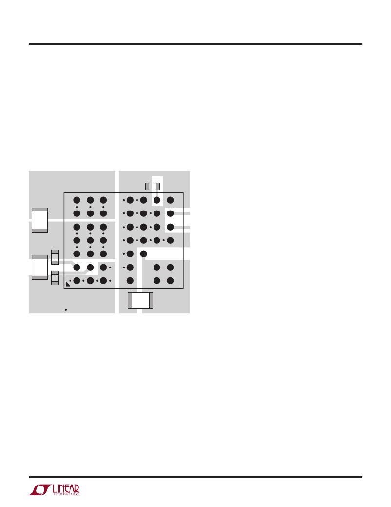
�PCBLayout�
�Most� of� the� headaches� associated� with� PCB� layout� have�
�been� alleviated� or� even� eliminated� by� the� high� level� of�
�integration� of� the� LTM8048.� The� LTM8048� is� neverthe-�
�less� a� switching� power� supply,� and� care� must� be� taken� to�
�minimize� electrical� noise� to� ensure� proper� operation.� Even�
�with� the� high� level� of� integration,� you� may� fail� to� achieve�
�specified� operation� with� a� haphazard� or� poor� layout.� See�
�Figure� 1� for� a� suggested� layout.� Ensure� that� the� grounding�
�and� heat� sinking� are� acceptable.�
�ADJ1�
�LTM8048�
�SS�
�BIAS�
�GND�
�V� OUT–�
�RUN�
�ADJ2� BYP�
�C� OUT2�
�V� OUT2� C� IN� V� IN�
�THERMAL/INTERCONNECT� VIAS�
�8048� F01�
�Figure� 1.� Layout� Showing� Suggested� External� Components,�
�Planes� and� Thermal� Vias�
�A� few� rules� to� keep� in� mind� are:�
�1.� Place� the� R� ADJ1� and� R� ADJ2� resistors� as� close� as� possible�
�to� their� respective� pins.�
�2.� Place� the� C� IN� capacitor� as� close� as� possible� to� the� V� IN�
�and� GND� connections� of� the� LTM8048.�
�3.� Place� the� C� OUT1� capacitor� as� close� as� possible� to� V� OUT1�
�and� V� OUT–� .� Likewise,� place� the� C� OUT2� capacitor� as� close�
�as� possible� to� V� OUT2� and� V� OUT–� .�
�4.� Place� the� C� IN� and� C� OUT� capacitors� such� that� their�
�ground� current� flow� directly� adjacent� or� underneath�
�the� LTM8048.�
�5.� Connect� all� of� the� GND� connections� to� as� large� a� copper�
�pour� or� plane� area� as� possible� on� the� top� layer.� Avoid�
�breaking� the� ground� connection� between� the� external�
�components� and� the� LTM8048.�
�6.� Use� vias� to� connect� the� GND� copper� area� to� the� board’s�
�internal� ground� planes.� Liberally� distribute� these� GND�
�vias� to� provide� both� a� good� ground� connection� and�
�thermal� path� to� the� internal� planes� of� the� printed� circuit�
�board.� Pay� attention� to� the� location� and� density� of� the�
�thermal� vias� in� Figure� 1.� The� LTM8048� can� benefit� from�
�the� heat� sinking� afforded� by� vias� that� connect� to� internal�
�GND� planes� at� these� locations,� due� to� their� proximity�
�to� internal� power� handling� components.� The� optimum�
�number� of� thermal� vias� depends� upon� the� printed�
�circuit� board� design.� For� example,� a� board� might� use�
�very� small� via� holes.� It� should� employ� more� thermal�
�vias� than� a� board� that� uses� larger� holes.�
�Hot-Plugging� Safely�
�The� small� size,� robustness� and� low� impedance� of� ceramic�
�capacitors� make� them� an� attractive� option� for� the� input�
�bypass� capacitor� of� the� LTM8048.� However,� these� capaci-�
�tors� can� cause� problems� if� the� LTM8048� is� plugged� into� a�
�live� supply� (see� Linear� Technology� Application� Note� 88� for�
�a� complete� discussion).� The� low� loss� ceramic� capacitor�
�combined� with� stray� inductance� in� series� with� the� power�
�source� forms� an� underdamped� tank� circuit,� and� the� volt-�
�age� at� the� V� IN� pin� of� the� LTM8048� can� ring� to� more� than�
�twice� the� nominal� input� voltage,� possibly� exceeding� the�
�LTM8048’s� rating� and� damaging� the� part.� A� similar� phe-�
�nomenon� can� occur� inside� the� LTM8048� module,� at� the�
�output� of� the� integrated� EMI� filter,� with� the� same� potential�
�of� damaging� the� part.� If� the� input� supply� is� poorly� con-�
�trolled� or� the� user� will� be� plugging� the� LTM8048� into� an�
�energized� supply,� the� input� network� should� be� designed�
�to� prevent� this� overshoot.� This� can� be� accomplished� by�
�installing� a� small� resistor� in� series� to� V� IN� ,� but� the� most�
�popular� method� of� controlling� input� voltage� overshoot� is�
�adding� an� electrolytic� bulk� capacitor� to� the� V� IN� or� f� IN� net.�
�This� capacitor’s� relatively� high� equivalent� series� resistance�
�damps� the� circuit� and� eliminates� the� voltage� overshoot.�
�The� extra� capacitor� improves� low� frequency� ripple� filter-�
�ing� and� can� slightly� improve� the� efficiency� of� the� circuit,�
�though� it� can� be� a� large� component� in� the� circuit.�
�8048ff�
�For� more� information� www.linear.com/LTM8048�
�13�
�相关PDF资料 |
PDF描述 |
|---|---|
| GMM43DRYI-S13 | CONN EDGECARD 86POS .156 EXTEND |
| RSO-1205S | CONV DC/DC 1W SNGL 5V OUT SIP8 |
| RSO-1212S | CONV DC/DC 1W 9-18VIN 12VOUT |
| REC3-0505SR/H1 | CONV DC/DC 3W 5VIN 05VOUT |
| MC78L15ABPRP | IC REG LDO 15V .1A TO-92 |
相关代理商/技术参数 |
参数描述 |
|---|---|
| LTM8048IY#PBF | 功能描述:IC DC/DC UMODULE LDO BGA RoHS:是 类别:电源 - 板载 >> DC DC Converters 系列:µModule® 设计资源:VI-200, VI-J00 Design Guide, Appl Manual 标准包装:1 系列:* 类型:隔离 输出数:1 电压 - 输入(最小):100V 电压 - 输入(最大):200V Voltage - Output 1:7.5V Voltage - Output 2:- Voltage - Output 3:- 电流 - 输出(最大):* 电源(瓦) - 制造商系列:100W 电压 - 隔离:* 特点:* 安装类型:通孔 封装/外壳:9-SlimMod 尺寸/尺寸:4.60" L x 1.80" W x 0.52" H(116.8mm x 45.7mm x 13.2mm) 包装:散装 工作温度:-25°C ~ 85°C 效率:* 电源(瓦特)- 最大:* |
| LTM8048IY#PBF | 制造商:Linear Technology 功能描述:DC/DC CONVERTER ISOLATED FB UMODULE BG |
| LTM8048MPY#PBF | 功能描述:IC DC/DC UMODULE LDO BGA RoHS:是 类别:电源 - 板载 >> DC DC Converters 系列:µModule® 设计资源:VI-200, VI-J00 Design Guide, Appl Manual 3D 型号:VI-Jxx-xx-F4.stp VI-Jxx-xx-F4.pdf 标准包装:1 系列:* 类型:隔离 输出数:1 电压 - 输入(最小):18V 电压 - 输入(最大):36V Voltage - Output 1:28V Voltage - Output 2:- Voltage - Output 3:- 电流 - 输出(最大):* 电源(瓦) - 制造商系列:25W 电压 - 隔离:* 特点:* 安装类型:通孔 封装/外壳:9 针半砖 FinMod 尺寸/尺寸:2.28" L x 1.86" W x 1.04" H(57.9mm x 47.2mm x 26.4mm) 包装:散装 工作温度:-10°C ~ 100°C 效率:* 电源(瓦特)- 最大:* |
| LTM8048MPY#PBF | 制造商:Linear Technology 功能描述:DC/DC CONVERTER ISOLATED FB UMODULE BG 制造商:Linear Technology 功能描述:DC/DC CONVERTER, ISOLATED FB UMODULE, BG |
| LTM8050EY#PBF | 制造商:Linear Technology 功能描述:DC/DC CONVERTER 0.8-24V 48W 制造商:Linear Technology 功能描述:BUCK UMODULE 58VIN 2A 2.4M 制造商:Linear Technology 功能描述:BUCK, UMODULE, 58VIN, 2A, 2.4MHZ, BGA-70 制造商:Linear Technology 功能描述:DC-DC REGULATOR, BUCK, ADJ, BGA-70, Primary Input Voltage:58V, No. of Outputs:1, 制造商:Linear Technology 功能描述:DC-DC REGULATOR, BUCK, ADJ, BGA-70, Primary Input Voltage:58V, No. of Outputs:1, Output Current:2A, No. of Pins:70, Operating Temperature Min:-40C, Operating Temperature Max:125C, MSL:MSL 3 - 168 hours, Package / Case:70-BGA , RoHS Compliant: Yes |
发布紧急采购,3分钟左右您将得到回复。