- 您现在的位置:买卖IC网 > PDF目录8720 > LV810RILFT (IDT, Integrated Device Technology Inc)IC CLK BUFF 1:10 133MHZ 20-QSOP PDF资料下载
参数资料
| 型号: | LV810RILFT |
| 厂商: | IDT, Integrated Device Technology Inc |
| 文件页数: | 8/14页 |
| 文件大小: | 0K |
| 描述: | IC CLK BUFF 1:10 133MHZ 20-QSOP |
| 产品培训模块: | Clock Distibution and Generation 1.0 |
| 标准包装: | 2,500 |
| 类型: | 扇出缓冲器(分配) |
| 电路数: | 1 |
| 比率 - 输入:输出: | 1:10 |
| 差分 - 输入:输出: | 无/无 |
| 输入: | 时钟 |
| 输出: | TTL |
| 频率 - 最大: | 133MHz |
| 电源电压: | 1.425 V ~ 2.625 V |
| 工作温度: | -40°C ~ 85°C |
| 安装类型: | 表面贴装 |
| 封装/外壳: | 20-SSOP(0.154",3.90mm 宽) |
| 供应商设备封装: | 20-QSOP |
| 包装: | 带卷 (TR) |
ICSLV810
BUFFER/CLOCK DRIVER
FAN OUT BUFFER
IDT / ICS BUFFER/CLOCK DRIVER
3
ICSLV810
REV H 051310
External Components
The ICSLV810 requires a minimum number of external
components for proper operation.
Decoupling Capacitors
Decoupling capacitors of 0.01F must be connected
between VDD and GND, as close to these pins as possible.
For optimum device performance, the decoupling capacitors
should be mounted on the component side of the PCB.
Avoid the use of vias in the decoupling circuit.
Series Termination Resistor
When the PCB trace between the clock outputs and the
loads are over 1 inch, series termination should be used. To
series terminate a 50
trace (a commonly used trace
impedance) place a 33
resistor in series with the clock line,
as close to the clock output pin as possible. The nominal
impedance of the clock output is 20
.
PCB Layout Recommendations
For optimum device performance and lowest output phase
noise, the following guidelines should be observed.
1) The 0.01F decoupling capacitors should be mounted on
the component side of the board as close to the VDD pins
as possible. No vias should be used between the
decoupling capacitors and VDD pins. The PCB trace to VDD
pin should be kept as short as possible, as should the PCB
trace to the ground via.
2) To minimize EMI the 33
series termination resistor, if
needed, should be placed close to the clock output.
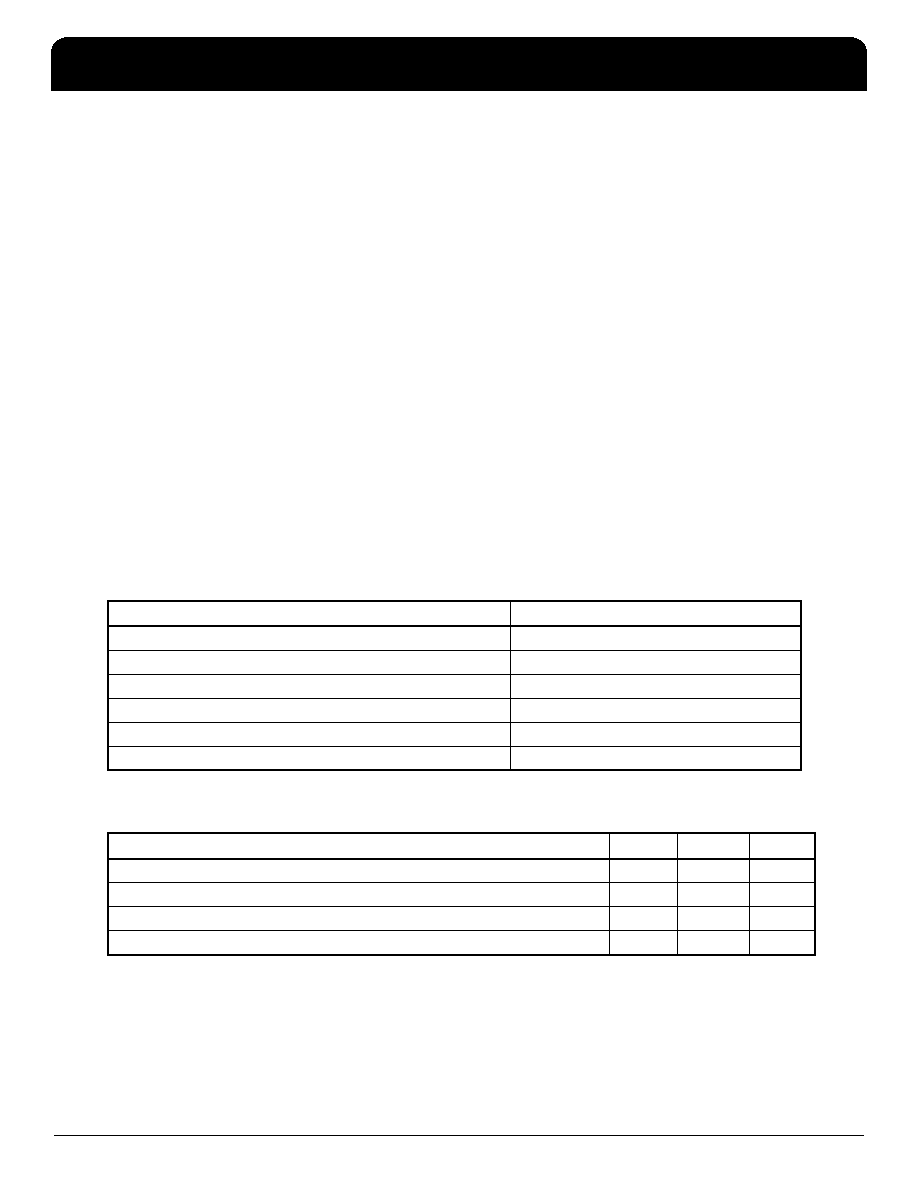
Absolute Maximum Ratings
Stresses above the ratings listed below can cause permanent damage to the ICSLV810. These ratings, which are
standard values for ICS commercially rated parts, are stress ratings only. Functional operation of the device at
these or any other conditions above those indicated in the operational sections of the specifications is not implied.
Exposure to absolute maximum rating conditions for extended periods can affect product reliability. Electrical
parameters are guaranteed only over the recommended operating temperature range.
Recommended Operation Conditions
Item
Rating
Supply Voltage, VDD MAX
7 V
All Inputs and Outputs
-0.5 V to VDDA + 1.2 V
Ambient Operating Temperature
-40 to +85
° C
Storage Temperature
-65 to +150
° C
Junction Temperature
125
° C
Soldering Temperature
260
° C
Parameter
Min.
Typ.
Max.
Units
Ambient Operating Temperature
-40
+85
° C
Power Supply Voltage (measured with respect to GND), VDDA
1.425
2.625
V
Power Supply Voltage (measured with respect to GND), VDDB
1.425
2.625
V
Power Supply Voltage (measured with respect to GND), VDDC
1.425
2.625
V
相关PDF资料 |
PDF描述 |
|---|---|
| LTC2641CMS8-12#PBF | IC DAC 12BIT VOUT 8-MSOP |
| LTC2641CDD-12#PBF | IC DAC 12BIT VOUT 8-DFN |
| SL2304NZZC-1Z | IC BUFFER 140MHZ 4CH 3.3V 8TSSOP |
| SL2304NZZC-1 | IC BUFFER 140MHZ 4CH 3.3V 8TSSOP |
| SL2304NZZC-1ZT | IC BUFFER 140MHZ 4CH 3.3V 8TSSOP |
相关代理商/技术参数 |
参数描述 |
|---|---|
| LV810RIT | 功能描述:IC CLK BUFF 1:10 133MHZ 20-QSOP RoHS:否 类别:集成电路 (IC) >> 时钟/计时 - 时钟缓冲器,驱动器 系列:- 标准包装:1 系列:HiPerClockS™ 类型:扇出缓冲器(分配),多路复用器 电路数:1 比率 - 输入:输出:2:18 差分 - 输入:输出:是/无 输入:CML,LVCMOS,LVPECL,LVTTL,SSTL 输出:LVCMOS,LVTTL 频率 - 最大:250MHz 电源电压:2.375 V ~ 3.465 V 工作温度:0°C ~ 70°C 安装类型:表面贴装 封装/外壳:32-LQFP 供应商设备封装:32-TQFP(7x7) 包装:- 其它名称:800-1923-6 |
| LV8111V | 制造商:SANYO 制造商全称:Sanyo Semicon Device 功能描述:For Polygon Mirror Motor 3-phase Brushless Motor Driver |
| LV8111V_0910 | 制造商:SANYO 制造商全称:Sanyo Semicon Device 功能描述:For Polygon Mirror Motor 3-phase Brushless Motor Driver |
| LV8111V_12 | 制造商:SANYO 制造商全称:Sanyo Semicon Device 功能描述:For Polygon Mirror Motor 3-phase Brushless Motor Driver |
| LV8111V-MPB-H | 功能描述:马达/运动/点火控制器和驱动器 RoHS:否 制造商:STMicroelectronics 产品:Stepper Motor Controllers / Drivers 类型:2 Phase Stepper Motor Driver 工作电源电压:8 V to 45 V 电源电流:0.5 mA 工作温度:- 25 C to + 125 C 安装风格:SMD/SMT 封装 / 箱体:HTSSOP-28 封装:Tube |
发布紧急采购,3分钟左右您将得到回复。