- 您现在的位置:买卖IC网 > PDF目录45007 > LX1662CDT 1.5 A SWITCHING CONTROLLER, 200 kHz SWITCHING FREQ-MAX, PDSO14 PDF资料下载
参数资料
| 型号: | LX1662CDT |
| 元件分类: | 稳压器 |
| 英文描述: | 1.5 A SWITCHING CONTROLLER, 200 kHz SWITCHING FREQ-MAX, PDSO14 |
| 封装: | PLASTIC, SOIC-14 |
| 文件页数: | 6/15页 |
| 文件大小: | 308K |
| 代理商: | LX1662CDT |
SINGLE-CHIP PROGRAMMABLE PWM CONTROLLERS WITH 5-BIT DAC
LX1662/62A, LX1663/63A
PRODUCT DA T ABOOK 1996/1997
Copyright 1999
Rev. 1.1 11/99
14
P RODUCTION D ATA S HEET
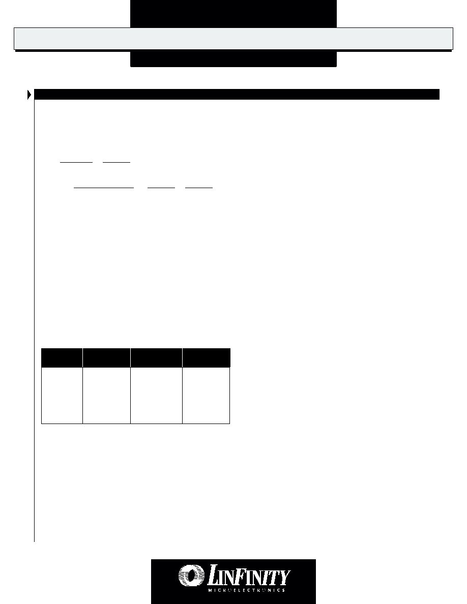
Device
R
DS(ON) @
I
D @
Max. Break-
10V (m
)T
C = 100°C
down Voltage
IRL3803
6
83
30
IRL22203N
7
71
30
IRL3103
14
40
30
IRL3102
13
56
20
IRL3303
26
24
30
IRL2703
40
17
30
TABLE 4 - FET Selection Guide
This table gives selection of suitable FETs from International Rectifier.
All devices in TO-220 package. For surface mount devices (TO-263 /
D2-Pak), add 'S' to part number, e.g. IRL3103S.
USING THE LX1662/63 DEVICES
CURRENT LIMIT (continued)
In cases where R
L is so large that the trip point current would
be lower than the desired short-circuit current limit, a resistor (R
S2)
can be put in parallel with C
S, as shown in Figure 11. The selection
of components is as follows:
=
C
S =
=
*
Again, select (R
S2//RS) < 10k.
FET SELECTION
To insure reliable operation, the operating junction temperature
of the FET switches must be kept below certain limits. The Intel
specification states that 115°C maximum junction temperature
should be maintained with an ambient of 50°C. This is achieved
by properly derating the part, and by adequate heat sinking. One
of the most critical parameters for FET selection is the R
DS ON
resistance.
This parameter directly contributes to the power
dissipation of the FET devices, and thus impacts heat sink design,
mechanical layout, and reliability.
In general, the larger the
current handling capability of the FET, the lower the R
DS ON will
be, since more die area is available.
FET SELECTION (continued)
For the IRL3102 (13m
R
DS(ON)), converting 5V to 2.8V at 14A
will result in typical heat dissipation of 1.48W.
Synchronous Rectification – Lower MOSFET
The lower pass element can be either a MOSFET or a Schottky
diode. The use of a MOSFET (synchronous rectification) will result
in higher efficiency, but at higher cost than using a Schottky diode
(non-synchronous).
Power dissipated in the bottom MOSFET will be:
P
D = I
2 * R
DS(ON) * [1 - Duty Cycle] = 2.24W
[IRL3303 or 1.12W for the IRL3102]
Catch Diode – Lower MOSFET
A low-power Schottky diode, such as a 1N5817, is recommended
to be connected between the gate and source of the lower
MOSFET when operating from a 12V-power supply (see Figure 9).
This will help protect the controller IC against latch-up due to the
inductor voltage going negative. Although latch-up is unlikely, the
use of such a catch diode will improve reliability and is highly
recommended.
Non-Synchronous Operation - Schottky Diode
A typical Schottky diode, with a forward drop of 0.6V will dissipate
0.6* 14* [1 – 2.8/5] = 3.7W (compared to the 1.1 to 2.2W dissipated
by a MOSFET under the same conditions). This power loss
becomes much more significant at lower duty cycles – synchro-
nous rectification is recommended especially when a 12V-power
input is used. The use of a dual Schottky diode in a single TO-220
package (e.g. the MBR2535) helps improve thermal dissipation.
MOSFET GATE BIAS
The power MOSFETs can be biased by one of two methods:
charge pump or 12V supply connected to V
C1.
1) Charge Pump (Bootstrap)
When 12V is supplied to the drain of the MOSFET, as in
Figure 9, the gate drive needs to be higher than 12V in order
to turn the MOSFET on. Capacitor C
10 and diodes D2 & D3
are used as a charge pump voltage doubling circuit to raise
the voltage of V
C1 so that the TDRV pin always provides a
high enough voltage to turn on Q
1.
The 12V supply must
always be connected to V
CC to provide power for the IC
itself, as well as gate drive for the bottom MOSFET.
2) 12V Supply
When 5V is supplied to the drain of Q
1, a 12V supply should
be connected to both V
CC and VC1.
R
L (Required)
R
L (Actual)
R
S2
R
S2 + RS
L
R
L (Actual) * (RS2 // RS)
L
R
L (Actual)
R
S + RS2
R
S2 * RS
The recommended solution is to use IRL3102 for the high side
and IRL3303 for the low side FET, for the best combination of cost
and performance. Alternative FET’s from any manufacturer could
be used, provided they meet the same criteria for R
DS(ON).
Heat Dissipated In Upper MOSFET
The heat dissipated in the top MOSFET will be:
P
D = (I
2 * R
DS(ON) * Duty Cycle) + (0.51 * VIN * tSW * fS )
Where t
SW is switching transition line for body diode (~100ns)
and f
S is the switching frequency.
相关PDF资料 |
PDF描述 |
|---|---|
| LX1663CDT | 1.5 A SWITCHING CONTROLLER, 200 kHz SWITCHING FREQ-MAX, PDSO16 |
| LX1663ACDT | 1.5 A SWITCHING CONTROLLER, 200 kHz SWITCHING FREQ-MAX, PDSO16 |
| LX1662ACD | 1.5 A SWITCHING CONTROLLER, 200 kHz SWITCHING FREQ-MAX, PDSO14 |
| LX1662CD | 1.5 A SWITCHING CONTROLLER, 200 kHz SWITCHING FREQ-MAX, PDSO14 |
| LX1662CN | 1.5 A SWITCHING CONTROLLER, 200 kHz SWITCHING FREQ-MAX, PDIP14 |
相关代理商/技术参数 |
参数描述 |
|---|---|
| LX1662CN | 功能描述:IC PWM PROG SGL 5BIT DAC 14 DIP RoHS:是 类别:集成电路 (IC) >> PMIC - 稳压器 - 专用型 系列:- 产品培训模块:Lead (SnPb) Finish for COTS Obsolescence Mitigation Program 标准包装:2,000 系列:- 应用:电源,ICERA E400,E450 输入电压:4.1 V ~ 5.5 V 输出数:10 输出电压:可编程 工作温度:-40°C ~ 85°C 安装类型:表面贴装 封装/外壳:42-WFBGA,WLCSP 供应商设备封装:42-WLP 包装:带卷 (TR) |
| LX1663 | 制造商:MICROSEMI 制造商全称:Microsemi Corporation 功能描述:SINGLE-CHIP PROGRAMMABLE PWM CONTROLLERS WITH 5-BIT DAC |
| LX1663A | 制造商:MICROSEMI 制造商全称:Microsemi Corporation 功能描述:SINGLE-CHIP PROGRAMMABLE PWM CONTROLLERS WITH 5-BIT DAC |
| LX1663ACD | 功能描述:IC PWM PROG SGL 5BIT DAC 16SOIC RoHS:是 类别:集成电路 (IC) >> PMIC - 稳压器 - 专用型 系列:- 产品培训模块:Lead (SnPb) Finish for COTS Obsolescence Mitigation Program 标准包装:2,000 系列:- 应用:电源,ICERA E400,E450 输入电压:4.1 V ~ 5.5 V 输出数:10 输出电压:可编程 工作温度:-40°C ~ 85°C 安装类型:表面贴装 封装/外壳:42-WFBGA,WLCSP 供应商设备封装:42-WLP 包装:带卷 (TR) |
| LX1663ACN | 功能描述:IC PWM PROG SGL 5BIT DAC 16DIP RoHS:是 类别:集成电路 (IC) >> PMIC - 稳压器 - 专用型 系列:- 产品培训模块:Lead (SnPb) Finish for COTS Obsolescence Mitigation Program 标准包装:2,000 系列:- 应用:电源,ICERA E400,E450 输入电压:4.1 V ~ 5.5 V 输出数:10 输出电压:可编程 工作温度:-40°C ~ 85°C 安装类型:表面贴装 封装/外壳:42-WFBGA,WLCSP 供应商设备封装:42-WLP 包装:带卷 (TR) |
发布紧急采购,3分钟左右您将得到回复。