- 您现在的位置:买卖IC网 > PDF目录45007 > LX1662CDT 1.5 A SWITCHING CONTROLLER, 200 kHz SWITCHING FREQ-MAX, PDSO14 PDF资料下载
参数资料
| 型号: | LX1662CDT |
| 元件分类: | 稳压器 |
| 英文描述: | 1.5 A SWITCHING CONTROLLER, 200 kHz SWITCHING FREQ-MAX, PDSO14 |
| 封装: | PLASTIC, SOIC-14 |
| 文件页数: | 7/15页 |
| 文件大小: | 308K |
| 代理商: | LX1662CDT |
SINGLE-CHIP PROGRAMMABLE PWM CONTROLLERS WITH 5-BIT DAC
LX1662/62A, LX1663/63A
PRODUCT DA T ABOOK 1996/1997
15
Copyright 1999
Rev. 1.1 11/99
P RODUCTION D ATA S HEET
Pentium is a registered trademark of Intel Corporation.
Cyrix is a registered trademark and 6x86, Gx86 and M2 are trademarks of Cyrix Corporation. K6 is a trademark of AMD.
Power PC is a trademark of International Business Machines Corporation. Alpha is a trademark of Digital Equipment Corporation.
USING THE LX1662/63 DEVICES
LAYOUT GUIDELINES - THERMAL DESIGN
A great deal of time and effort were spent optimizing the thermal
design of the demo boards. Any user who intends to implement
an embedded motherboard would be well advised to carefully
read and follow these guidelines. If the FET switches have been
carefully selected, external heatsinking is generally not required.
However, this means that copper trace on the PC board must now
be used. This is a potential trouble spot; as much copper area as
possible must be dedicated to heatsinking the FET switches, and
the diode as well if a non-synchronous solution is used.
In our VRM module, heatsink area was taken from internal
ground and V
CC planes which were actually split and connected
with VIAS to the power device tabs. The TO-220 and TO-263
cases are well suited for this application, and are the preferred
packages. Remember to remove any conformal coating from all
exposed PC traces which are involved in heatsinking.
General Notes
As always, be sure to provide local capacitive decoupling close to
the chip. Be sure use ground plane construction for all high-
frequency work. Use low ESR capacitors where justified, but be
alert for damping and ringing problems. High-frequency designs
demand careful routing and layout, and may require several
iterations to achieve desired performance levels.
Power Traces
To reduce power losses due to ohmic resistance, careful consid-
eration should be given to the layout of traces that carry high
currents. The main paths to consider are:
I Input power from 5V supply to drain of top MOSFET.
I Trace between top MOSFET and lower MOSFET or Schottky
diode.
I Trace between lower MOSFET or Schottky diode and
ground.
I Trace between source of top MOSFET and inductor, sense
resistor and load.
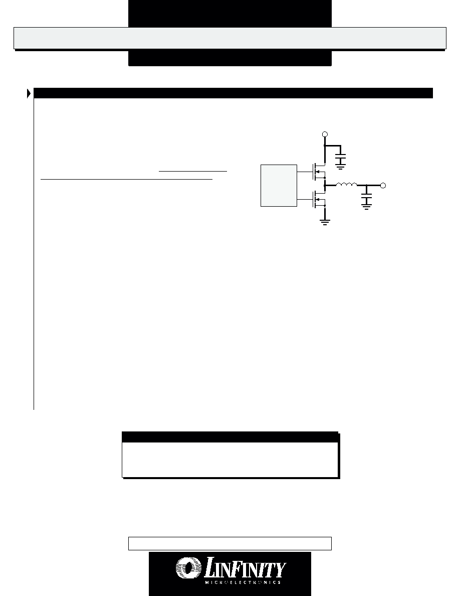
FIGURE 13 — Power Traces
Output
Input
5V or 12V
LX166x
All of these traces should be made as wide and thick as
possible, in order to minimize resistance and hence power losses.
It is also recommended that, whenever possible, the ground, input
and output power signals should be on separate planes (PCB
layers). See Figure 13 – bold traces are power traces.
C
5 Input Decoupling (VCC) Capacitor
Ensure that this 1F capacitor is placed as close to the IC as
possible to minimize the effects of noise on the device.
Layout Assistance
Please contact Linfinity’s Applications Engineers for assistance
with any layout or component selection issues. A Gerber file
with layout for the most popular devices is available upon re-
quest.
Evaluation boards are also available upon request. Please
check Linfinity's web site for further application notes.
PRODUCTION DATA - Information contained in this document is proprietary to LinFinity, and is current as of publication date. This document
may not be modified in any way without the express written consent of LinFinity. Product processing does not necessarily include testing of
all parameters. Linfinity reserves the right to change the configuration and performance of the product and to discontinue product at any time.
RELA TED DEVICES
LX1664/1665 - Dual Output PWM for Processor Applications
LX1668 - Triple Output PWM for Processor Applications
LX1553 - PWM for 5V - 3.3V Conversion
相关PDF资料 |
PDF描述 |
|---|---|
| LX1663CDT | 1.5 A SWITCHING CONTROLLER, 200 kHz SWITCHING FREQ-MAX, PDSO16 |
| LX1663ACDT | 1.5 A SWITCHING CONTROLLER, 200 kHz SWITCHING FREQ-MAX, PDSO16 |
| LX1662ACD | 1.5 A SWITCHING CONTROLLER, 200 kHz SWITCHING FREQ-MAX, PDSO14 |
| LX1662CD | 1.5 A SWITCHING CONTROLLER, 200 kHz SWITCHING FREQ-MAX, PDSO14 |
| LX1662CN | 1.5 A SWITCHING CONTROLLER, 200 kHz SWITCHING FREQ-MAX, PDIP14 |
相关代理商/技术参数 |
参数描述 |
|---|---|
| LX1662CN | 功能描述:IC PWM PROG SGL 5BIT DAC 14 DIP RoHS:是 类别:集成电路 (IC) >> PMIC - 稳压器 - 专用型 系列:- 产品培训模块:Lead (SnPb) Finish for COTS Obsolescence Mitigation Program 标准包装:2,000 系列:- 应用:电源,ICERA E400,E450 输入电压:4.1 V ~ 5.5 V 输出数:10 输出电压:可编程 工作温度:-40°C ~ 85°C 安装类型:表面贴装 封装/外壳:42-WFBGA,WLCSP 供应商设备封装:42-WLP 包装:带卷 (TR) |
| LX1663 | 制造商:MICROSEMI 制造商全称:Microsemi Corporation 功能描述:SINGLE-CHIP PROGRAMMABLE PWM CONTROLLERS WITH 5-BIT DAC |
| LX1663A | 制造商:MICROSEMI 制造商全称:Microsemi Corporation 功能描述:SINGLE-CHIP PROGRAMMABLE PWM CONTROLLERS WITH 5-BIT DAC |
| LX1663ACD | 功能描述:IC PWM PROG SGL 5BIT DAC 16SOIC RoHS:是 类别:集成电路 (IC) >> PMIC - 稳压器 - 专用型 系列:- 产品培训模块:Lead (SnPb) Finish for COTS Obsolescence Mitigation Program 标准包装:2,000 系列:- 应用:电源,ICERA E400,E450 输入电压:4.1 V ~ 5.5 V 输出数:10 输出电压:可编程 工作温度:-40°C ~ 85°C 安装类型:表面贴装 封装/外壳:42-WFBGA,WLCSP 供应商设备封装:42-WLP 包装:带卷 (TR) |
| LX1663ACN | 功能描述:IC PWM PROG SGL 5BIT DAC 16DIP RoHS:是 类别:集成电路 (IC) >> PMIC - 稳压器 - 专用型 系列:- 产品培训模块:Lead (SnPb) Finish for COTS Obsolescence Mitigation Program 标准包装:2,000 系列:- 应用:电源,ICERA E400,E450 输入电压:4.1 V ~ 5.5 V 输出数:10 输出电压:可编程 工作温度:-40°C ~ 85°C 安装类型:表面贴装 封装/外壳:42-WFBGA,WLCSP 供应商设备封装:42-WLP 包装:带卷 (TR) |
发布紧急采购,3分钟左右您将得到回复。