- 您现在的位置:买卖IC网 > PDF目录67759 > LX1732CDUT (MICROSEMI CORP-ANALOG MIXED SIGNAL GROUP) 1 A SWITCHING REGULATOR, 135 kHz SWITCHING FREQ-MAX, PDSO8 PDF资料下载
参数资料
| 型号: | LX1732CDUT |
| 厂商: | MICROSEMI CORP-ANALOG MIXED SIGNAL GROUP |
| 元件分类: | 稳压器 |
| 英文描述: | 1 A SWITCHING REGULATOR, 135 kHz SWITCHING FREQ-MAX, PDSO8 |
| 封装: | PLASTIC, MSOP-8 |
| 文件页数: | 10/12页 |
| 文件大小: | 450K |
| 代理商: | LX1732CDUT |
Microsemi
Integrated Products
11861 Western Avenue, Garden Grove, CA. 92841, 714-898-8121, Fax: 714-893-2570
Page 7
Copyright
2000
Rev. 1.1, 2003-07-29
WWW
.Microse
m
i
.CO
M
LX1732
High Current PFM Boost Converter
PRODUCTION DATA SHEET
I N T E GRA T ED
PR ODUC T S
EVALUATION BOA RD
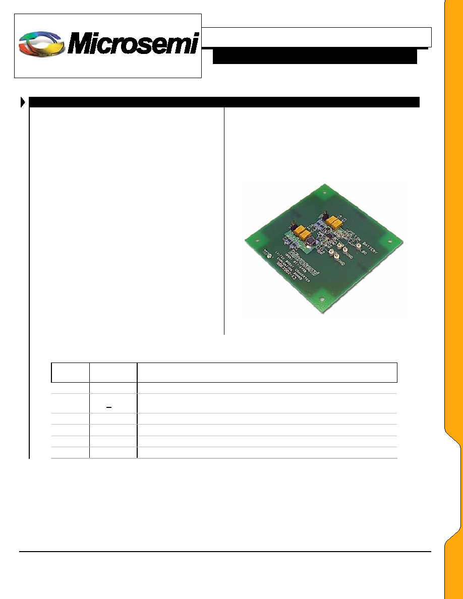
OVERVIEW
The LXE1732 evaluation board is available from
Microsemi for assessing overall circuit performance. The
evaluation board, shown in Figure 6, is 3 by 3 inches (i.e.,
7.6 X 7.6cm) square and factory calibrated for optimal
performance over a wide load range. Circuit designers can
easily modify output voltage to suit their particular
application. Moreover, inductor, capacitors, and diode are
easily swapped out to promote design verification of a
circuit that maximizes efficiency and minimizes cost for a
wide variety of applications.
The input and output
connections are described in Table 1.
ELECTRICAL CONNECTIONS
Apply the DC input voltage directly to the VIN pin and
connect the test load to the VOUT pin. The output voltage
is factory programmed at 3.0V, however, the user may
adjust this value by changing the R1 and R2 values
accordingly. Install a wire loop at JU1 to close the circuit
connection and to examine the inductor current using a
suitable current probe.
The LX1732 exhibits a low quiescent current (IQ <
1
A: typ) during shutdown mode. This pin is pulled-up to
VIN via a 10K resistor. Grounding the SHDN test point
shuts down the IC however, the load is still capable of
drawing current through the inductor & diode circuit path.
Hence, VOUT during shutdown will be approximately the
input voltage minus the inductor and diode forward voltage
drop.
The LXE1732 evaluation board provides an easy and
cost effective solution for evaluation of the LX1732. The
factory installed component list for the evaluation board is
provided in Table 2 and the schematic is shown in Figure 7.
Figure 6 – LX1732 Evaluation Board
Table 1: Input and Output Pin Assignments
Pin
Name
Allowable
Range
Description
VIN
0 to 6V
Input power supply connection.
LBI
V < VIN
Low Battery Input voltage threshold sense pin: Programmed for 0.93V
nominal.
LBO
N/A
Low Battery Output voltage: Connect a DVM to LBO to observe voltage.
/SHDN
0 to VIN
Ground to inhibit the LX1732
VOUT
V > VIN
Programmed for 3.0V nominal output, adjustable via R1 and R2.
GND
0V
Circuit Ground
EE
VV
AA
LL
UU
AA
TT
IIOO
NN
相关PDF资料 |
PDF描述 |
|---|---|
| LX1801CLQ | SPECIALTY ANALOG CIRCUIT, PQCC16 |
| LX1801CLQ-TR | SPECIALTY ANALOG CIRCUIT, PQCC16 |
| LY5150ALH | SPECIALTY ANALOG CIRCUIT, PBGA16 |
| LY5150ALHTR | SPECIALTY ANALOG CIRCUIT, PBGA16 |
| LZ34B1B | SPECIALTY ANALOG CIRCUIT, CQCC36 |
相关代理商/技术参数 |
参数描述 |
|---|---|
| LX1734 | 制造商:MICROSEMI 制造商全称:Microsemi Corporation 功能描述:1.0MHz Inverting DC/DC Converter |
| LX1734-01 EVAL KIT | 制造商:Microsemi Corporation 功能描述:DC:DC CONVERTER - Bulk |
| LX1734CLM | 功能描述:IC REG INV ADJ 0.75A 6MLPL RoHS:是 类别:集成电路 (IC) >> PMIC - 稳压器 - DC DC 开关稳压器 系列:- 标准包装:20 系列:SIMPLE SWITCHER® 类型:降压(降压) 输出类型:固定 输出数:1 输出电压:12V 输入电压:4 V ~ 60 V PWM 型:电压模式 频率 - 开关:52kHz 电流 - 输出:1A 同步整流器:无 工作温度:-40°C ~ 125°C 安装类型:通孔 封装/外壳:16-DIP(0.300",7.62mm) 包装:管件 供应商设备封装:16-DIP 其它名称:*LM2575HVN-12LM2575HVN-12 |
| LX1735 EVAL KIT | 制造商:Microsemi Corporation 功能描述:DC:DC CONVERTER - Bulk |
| LX1735CLD | 制造商:Microsemi Corporation 功能描述:PWM CONTROLLERS - Bulk |
发布紧急采购,3分钟左右您将得到回复。