- 您现在的位置:买卖IC网 > PDF目录45008 > LX1742CDU-TR (MICROSEMI CORP-ANALOG MIXED SIGNAL GROUP) SWITCHING REGULATOR, PDSO8 PDF资料下载
参数资料
| 型号: | LX1742CDU-TR |
| 厂商: | MICROSEMI CORP-ANALOG MIXED SIGNAL GROUP |
| 元件分类: | 稳压器 |
| 英文描述: | SWITCHING REGULATOR, PDSO8 |
| 封装: | PLASTIC, MSOP-8 |
| 文件页数: | 6/13页 |
| 文件大小: | 456K |
| 代理商: | LX1742CDU-TR |
Microsemi
Integrated Products Division
11861 Western Avenue, Garden Grove, CA. 92841, 714-898-8121, Fax: 714-893-2570
Page 2
Copyright
2000
Rev. 1.0b, 2005-03-03
WWW
.Microse
m
i
.CO
M
LX1742
High Efficiency High Voltage Boost Controller
PRODUCTION DATA SHEET
I N T E GRA T ED
PR ODUC T S
ABSOLUTE MAXI MUM RATI NGS
Supply Voltage (VIN) ..................................................................................... -0.3V to 7.0V
Output Voltage (OUT)................................................................................................25.0V
Feedback Input Voltage (VFB) ..............................................................-0.3V to VIN + 0.3V
Shutdown Input Voltage (VSHDN) ........................................................-0.3V to VIN + 0.3V
PWM Input Amplitude .........................................................................-0.3V to VIN + 0.3V
Analog Adjust Input Voltage (VADJ).................................................................-0.3V to VIN
Source Input Current (ISRC).................................................................................500mARMS
Operating Junction Temperature................................................................................ 150°C
Storage Temperature Range.........................................................................-65°C to 150°C
Peak Package Solder Reflow Temp. (40 second max. exposure).................. 260°C (+0, -5)
Note: Exceeding these ratings could cause damage to the device. All voltages are with respect to
Ground. Currents are positive into, negative out of specified terminal
.
TH ERM A L DATA
DU
Plastic MSOP 8-Pin
THERMAL RESISTANCE
-JUNCTION TO AMBIENT,
θJA
206
°C/W
THERMAL RESISTANCE
-JUNCTION TO CASE,
θJC
39
°C/W
Junction Temperature Calculation: TJ = TA + (PD x θJC). The θJA numbers are guidelines for the
thermal performance of the device/pc-board system. All of the above assume no ambient airflow.
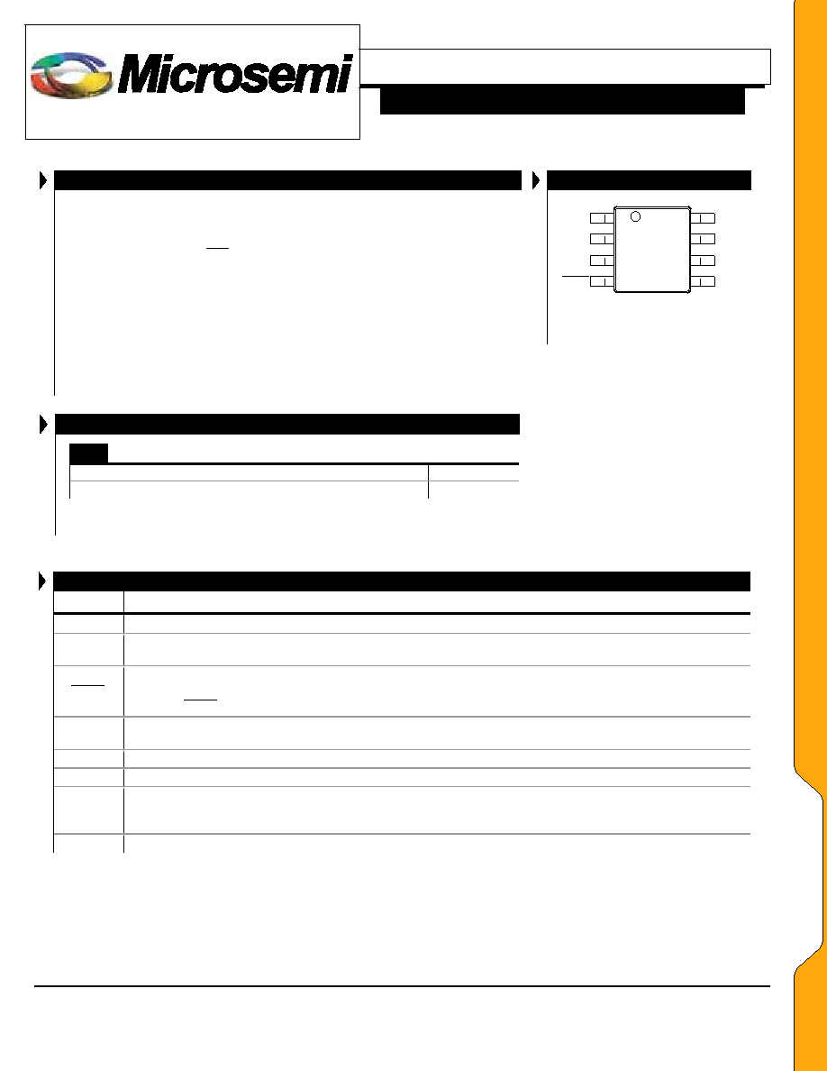
PACKAGE PIN OUT
1
2
4
3
5
6
8
7
SW
FB
IN
GND
OUT
CS
ADJ
DU PACKAGE
(Top View)
SHDN
RoHS / Pb-free 100% Matte Tin Lead Finish
FUNCTIONAL PIN DESCRIPTION
NAME
DESCRIPTION
IN
Unregulated IC Supply Voltage Input – Input range from +1.6V to 6.0V. Bypass with a 1F or greater capacitor.
FB
Feedback Input – Connect to a resistive divider network between the output and GND to set the output voltage between VCC
(IN) and 25V. The feedback threshold is 1.20V.
SHDN
Active-Low Shutdown Input – A logic low shuts down the device and reduces the supply current to 0.1A. When
shutdown, the LX1742 isolates the output from the input by turning off the internal MOSFET between LX and OUT.
Connect SHDN to VCC for normal operation.
SW
Inductor Switching Connection – Internally connected to the drain of a 28V N-channel MOSFET. LX is high impedance in
shutdown.
CS
Current-Sense Amplifier Input – Connecting a resistor between CS and GND sets the peak inductor current limit.
GND
Common terminal for ground reference.
ADJ
PWM Signal Input – Connects to the internal reference, via an internal filter and gain resistor, allowing a dynamic output
voltage adjustment ±15% in corresponding to a varying duty cycle. 50% duty cycle yields a nominal output set via the FB
pin (See Note) or ADJ input voltage range from 0.9V to 1.5V DC
OUT
Output voltage is adjustable up to 25V (maximum).
PP
AA
CC
KK
AA
GG
EE
DD
AA
TT
AA
相关PDF资料 |
PDF描述 |
|---|---|
| LX1823IQ | 2 A SWITCHING CONTROLLER, 1500 kHz SWITCHING FREQ-MAX, PQCC20 |
| LX1823IN | 2 A SWITCHING CONTROLLER, 1500 kHz SWITCHING FREQ-MAX, PDIP16 |
| LX1823IJ | 2 A SWITCHING CONTROLLER, 1500 kHz SWITCHING FREQ-MAX, CDIP16 |
| LX1823IJ | 2 A SWITCHING CONTROLLER, 1500 kHz SWITCHING FREQ-MAX, CDIP16 |
| LX1823MJ | 2 A SWITCHING CONTROLLER, 1500 kHz SWITCHING FREQ-MAX, CDIP16 |
相关代理商/技术参数 |
参数描述 |
|---|---|
| LX1742EVALKIT | 制造商:未知厂家 制造商全称:未知厂家 功能描述:DC:DC Converter |
| LX1744 | 制造商:MICROSEMI 制造商全称:Microsemi Corporation 功能描述:Dual Output Boost ? LED Driver / LCD Bias |
| LX1744 EVAL KIT | 制造商:Microsemi Corporation 功能描述:LED BACKLIGHT CONTROLLERS AND DRIVERS - Bulk |
| LX1744CLQ | 功能描述:IC LED DRVR WT/CLR BCKLGT 16MLPQ RoHS:是 类别:集成电路 (IC) >> PMIC - LED 驱动器 系列:- 产品培训模块:Lead (SnPb) Finish for COTS Obsolescence Mitigation Program 标准包装:2,500 系列:- 恒定电流:- 恒定电压:- 拓扑:升压(升压),切换式电容器(充电泵) 输出数:1 内部驱动器:是 类型 - 主要:背光 类型 - 次要:白色 LED 频率:625kHz ~ 875kHz 电源电压:2.7 V ~ 5.3 V 输出电压:5V 安装类型:表面贴装 封装/外壳:10-TFSOP,10-MSOP(0.118",3.00mm 宽) 供应商设备封装:10-µMAX 包装:带卷 (TR) 工作温度:-40°C ~ 85°C |
| LX1744CPW | 功能描述:IC LED DRVR WT/CLR BCKLT 14TSSOP RoHS:是 类别:集成电路 (IC) >> PMIC - LED 驱动器 系列:- 产品培训模块:Lead (SnPb) Finish for COTS Obsolescence Mitigation Program 标准包装:2,500 系列:- 恒定电流:- 恒定电压:- 拓扑:升压(升压),切换式电容器(充电泵) 输出数:1 内部驱动器:是 类型 - 主要:背光 类型 - 次要:白色 LED 频率:625kHz ~ 875kHz 电源电压:2.7 V ~ 5.3 V 输出电压:5V 安装类型:表面贴装 封装/外壳:10-TFSOP,10-MSOP(0.118",3.00mm 宽) 供应商设备封装:10-µMAX 包装:带卷 (TR) 工作温度:-40°C ~ 85°C |
发布紧急采购,3分钟左右您将得到回复。