- 您现在的位置:买卖IC网 > PDF目录95794 > LXM1621-04 (MICROSEMI CORP-ANALOG MIXED SIGNAL GROUP) SPECIALTY ANALOG CIRCUIT, XMA PDF资料下载
参数资料
| 型号: | LXM1621-04 |
| 厂商: | MICROSEMI CORP-ANALOG MIXED SIGNAL GROUP |
| 元件分类: | 模拟信号调理 |
| 英文描述: | SPECIALTY ANALOG CIRCUIT, XMA |
| 文件页数: | 4/10页 |
| 文件大小: | 280K |
| 代理商: | LXM1621-04 |
Microsemi
Linfinity Microelectronics Division
11861 Western Avenue, Garden Grove, CA. 92841, 714-898-8121, Fax: 714-893-2570
Page 3
Copyright
2000
Rev. 1.0a, 2005-02-07
WWW
.Microse
m
i
.CO
M
RangeMAX
LXM1621-xx
DIGITAL DIMMING DUAL LAMP CCFL INVERTER MODULE
PRODUCTION DATA SHEET
I N T E GRA T ED
PR ODUC T S
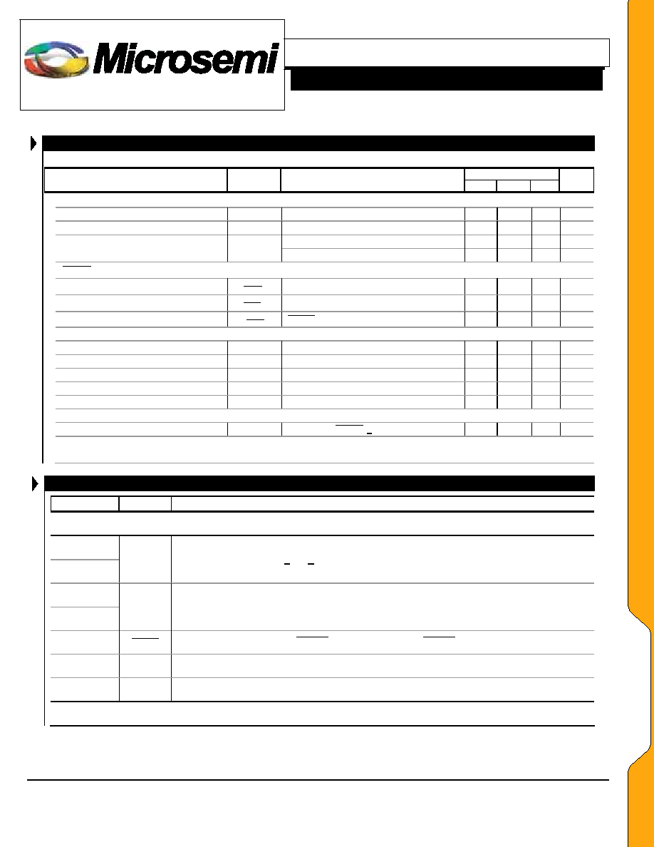
ELECTRI CAL CHA RACTERI STI CS (CONTINUED)
Unless otherwise specified, these specifications apply over the recommended operating conditions and 25°C ambient temperature for the LMX1621-xx.
LMX1621-xx
Parameter
Symbol
Test Conditions
Min
Typ
Max
Units
BRITE INPUT
Input Current
IBRT
VBRT_ADJ = 0V
-6
-8
-10
ADC
Input Voltage For Max. Lamp Current
VC
IO(LAMP) = 100% Duty Cycle
2.5
2.6
VDC
IO(LAMP) = 2% Duty Cycle
0
VDC
Input Voltage For Min. Lamp Current
(Note 3)
VC
IO(LAMP) = 0.5% Duty Cycle
-50
mVDC
SLEEP INPUT
RUN Mode
(HI)
SLEEP
V
2.2
VIN
VDC
SLEEP Mode
(LO)
SLEEP
V
-0.3
0.8
VDC
Input Current
SLEEP
I
SLEEP = 5.0V
70
75
100
ADC
VSYNC CHARACTERISTICS
Logic High Level
VSYNC(HI)
4.0
6.5
VDC
Logic Low Level
VSYNC(LO)
-0.3
1.0
VDC
Input Impedance
ZIN
60
66
75
K
Pulse Width (Note 4)
tPW
25
250
s
Input Frequency
fSYNC
49
150
Hz
POWER CHARACTERISTICS
Sleep Current
IIN(MIN)
VIN = 12VDC, SLEEP < 0.8V
5
50
ADC
Note 2: Minimum lamp current required to maintain even light output may vary with display panel.
Note 3: See 200:1 Dimming Application section for details.
Note 4: The module will be functional with pulse widths much larger than 250s.
FUNCTIONAL PIN DESCRIPTION
Conn.
Pin
Description
CN1
CN1-1
CN1-2
VIN
Input Power Supply (8V < VIN < 16V)
CN1-3
CN1-4
GND
Power Supply Return
CN1-5
SLEEP
ON / OFF Control. (2.2V < SLEEP < VIN = ON, -0.3V < SLEEP < 0.8V = OFF)
CN1-6
BRITE
Brightness Control (-0.3V to 2.5VDC). 2.5VDC gives maximum lamp current.
CN1-7, 8
VSYNC
Vertical synchronization input 49Hz < fSYNC < 150Hz
CN2 thru CN5: Refer to Connection Schematic Section
EE
LL
EE
CC
TT
RR
IICC
AA
LL
SS
相关PDF资料 |
PDF描述 |
|---|---|
| LZ2111J | SPECIALTY ANALOG CIRCUIT, CDIP20 |
| LZ2112J | SPECIALTY ANALOG CIRCUIT, CDIP20 |
| LZ2121J | SPECIALTY ANALOG CIRCUIT, CDIP20 |
| LZ2122J | SPECIALTY ANALOG CIRCUIT, CDIP20 |
| LZ22251 | SPECIALTY ANALOG CIRCUIT, CDIP22 |
相关代理商/技术参数 |
参数描述 |
|---|---|
| LXM1621-XX | 制造商:MICROSEMI 制造商全称:Microsemi Corporation 功能描述:DIGITAL DIMMING DUAL LAMP CCFL INVERTER MODULE |
| LXM1622-05-01 | 制造商:未知厂家 制造商全称:未知厂家 功能描述:CCFL Inverter Module - Dual Lamp |
| LXM1622-05-02 | 制造商:未知厂家 制造商全称:未知厂家 功能描述:CCFL Inverter Module - Dual Lamp |
| LXM1622-05-03 | 制造商:未知厂家 制造商全称:未知厂家 功能描述:CCFL Inverter Module - Dual Lamp |
| LXM1622-05-XX | 制造商:MICROSEMI 制造商全称:Microsemi Corporation 功能描述:DUAL 5W, DIGITAL DIMMING CCFL INVERTER MODULE |
发布紧急采购,3分钟左右您将得到回复。