- 您现在的位置:买卖IC网 > PDF目录369885 > LXT3108BE LINE INTERFACE|BGA|256PIN|PLASTIC PDF资料下载
参数资料
| 型号: | LXT3108BE |
| 英文描述: | LINE INTERFACE|BGA|256PIN|PLASTIC |
| 中文描述: | 线路接口|的BGA | 256PIN |塑料 |
| 文件页数: | 20/26页 |
| 文件大小: | 402K |
| 代理商: | LXT3108BE |
LXT310
—
T1 CSU/ISDN PRI Transceiver
20
Datasheet
4.0
Test Specifications
Note:
The minimum and maximum values in
Table 7
through
Table 14
and
Figure 9
through
Figure 13
represent the performance specifications of the LXT310 and are guaranteed by test, except where
noted by design
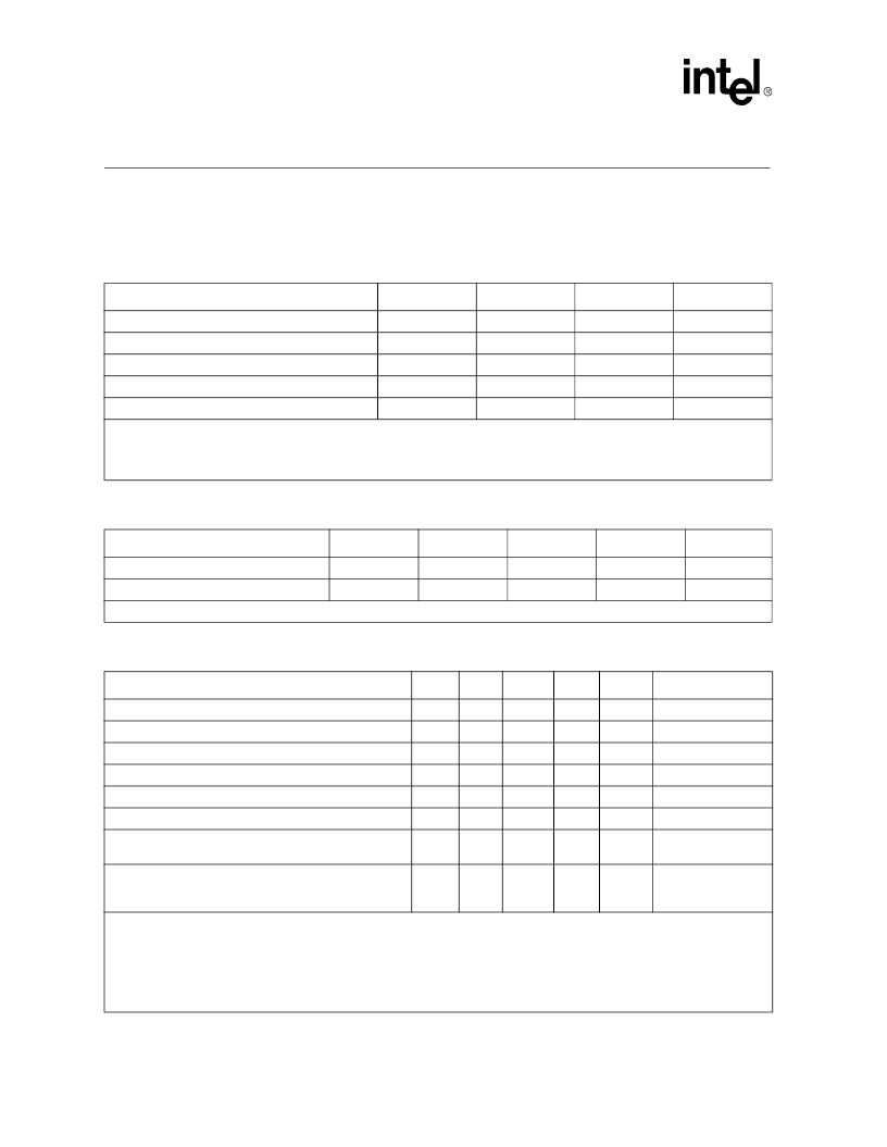
Table 7. Absolute Maximum Ratings
Parameter
Sym
Min
Max
Units
DC supply (referenced to GND)
RV+, TV+
-0.3
6.0
V
Input voltage, any pin
Input current, any pin
1
V
IN
RGND - 0.3
RV+ + 0.3
V
I
IN
-10
10
mA
Ambient operating temperature
T
A
-40
85
°
C
Storage temperature
T
STG
-65
150
°
C
Caution:
Operations at or beyond these limits may result in permanent damage to the device.
Normal operation is not guaranteed at these extremes.
1. Transient currents of up to 100 mA will not cause SCR latch up. TTIP, TRING, TV+ and TGND can withstand a continuous
current of 100 mA.
Table 8. Recommended Operating Conditions and Characteristics
Parameter
Sym
Min
Typ
Max
Units
DC supply
1
RV+, TV+
4.75
5.0
5.25
V
Ambient operating temperature
T
A
–
25
–
°
C
1. TV+ must not exceed RV+ by more than 0.3 V.
Table 9. Electrical Characteristics
(Under Recommended Operating Conditions)
Parameter
Sym
Min
Typ
1
Max
Units
Test Conditions
High level input voltage
2,3
(pins 1-5, 10, 23-28)
V
IH
2.0
–
–
V
Low level input voltage
2,3
(pins 1-5, 10, 23-28)
Vil
–
–
0.8
V
High level output voltage
2,3
(pins 6-8, 11, 12, 23, 25)
V
OH
2.4
–
–
V
I
OUT
= -400
μ
A
Low level output voltage
2,3
(pins 6-8, 11, 12, 23, 25)
V
OL
–
–
0.4
V
I
OUT
= 1.6 mA
Input leakage current
I
LL
0
–
±10
μ
A
Three-state leakage current
2
(pin 25)
I3
L
0
–
±10
μ
A
Driver power down current
4
IPD
–
–
±1.2
mA
Direct connection to
VCC or GND
Total power dissipation
5
P
D
–
620
–
mW
100% ones density &
maximum line length
@ 5.25 V
1. Typical values are measured at 25
°
C and are for design aid only; not guaranteed and not subject to production testing.
2. Functionality of pins 23 and 25 depends on mode. See Host/Hardware mode descriptions.
3. Output drivers will output CMOS logic levels into CMOS loads.
4. TTIP, TRING only in Idle or Power Down mode.
5. Power dissipation as shown in
Figure 8
while driving a 100
resistive load terminating transformer over operating
temperature range. Includes device and load. Digital input levels are within 10% of the supply rails and digital outputs are
driving a 50 pF capacitive load.
相关PDF资料 |
PDF描述 |
|---|---|
| LXT3108HE | LINE INTERFACE|QFP|208PIN|PLASTIC |
| LXT310JE | PCM Transceiver |
| LXT310NE | PCM TRANSCEIVER|SINGLE|T-1(DS1)|CMOS|DIP|28PIN|PLASTIC |
| LXT316NE | PCM Repeater |
| LXT316PE | PCM Repeater |
相关代理商/技术参数 |
参数描述 |
|---|---|
| LXT3108HE | 制造商:未知厂家 制造商全称:未知厂家 功能描述:LINE INTERFACE|QFP|208PIN|PLASTIC |
| LXT310JE | 制造商:未知厂家 制造商全称:未知厂家 功能描述:PCM Transceiver |
| LXT310NE | 制造商:LEVEL ONE 功能描述: |
| LXT310PE | 制造商:Intel 功能描述: 制造商:LEVEL_ONE 功能描述: 制造商:LEVEL ONE 功能描述:PCM TRANSCEIVER, Single, T-1(DS1), 28 Pin, Plastic, PLCC |
| LXT310PE-IJC8 | 制造商:LEVE ONE 功能描述:310PE-IJC8 |
发布紧急采购,3分钟左右您将得到回复。