- 您现在的位置:买卖IC网 > PDF目录369885 > LXT331PE LINE INTERFACE|CMOS|LDCC|44PIN|PLASTIC PDF资料下载
参数资料
| 型号: | LXT331PE |
| 英文描述: | LINE INTERFACE|CMOS|LDCC|44PIN|PLASTIC |
| 中文描述: | 线路接口|的CMOS | LDCC | 44PIN |塑料 |
| 文件页数: | 25/32页 |
| 文件大小: | 395K |
| 代理商: | LXT331PE |
第1页第2页第3页第4页第5页第6页第7页第8页第9页第10页第11页第12页第13页第14页第15页第16页第17页第18页第19页第20页第21页第22页第23页第24页当前第25页第26页第27页第28页第29页第30页第31页第32页
Dual T1/E1 Line Interface Unit
—
LXT331
Datasheet
25
4.0
Test Specifications
Note:
The minimum and maximum values in
Table 8
through
Table 14
and
Figure 14
through
Figure 17
represent the performance specifications of the LXT331 and are guaranteed by test, except where
noted by design.
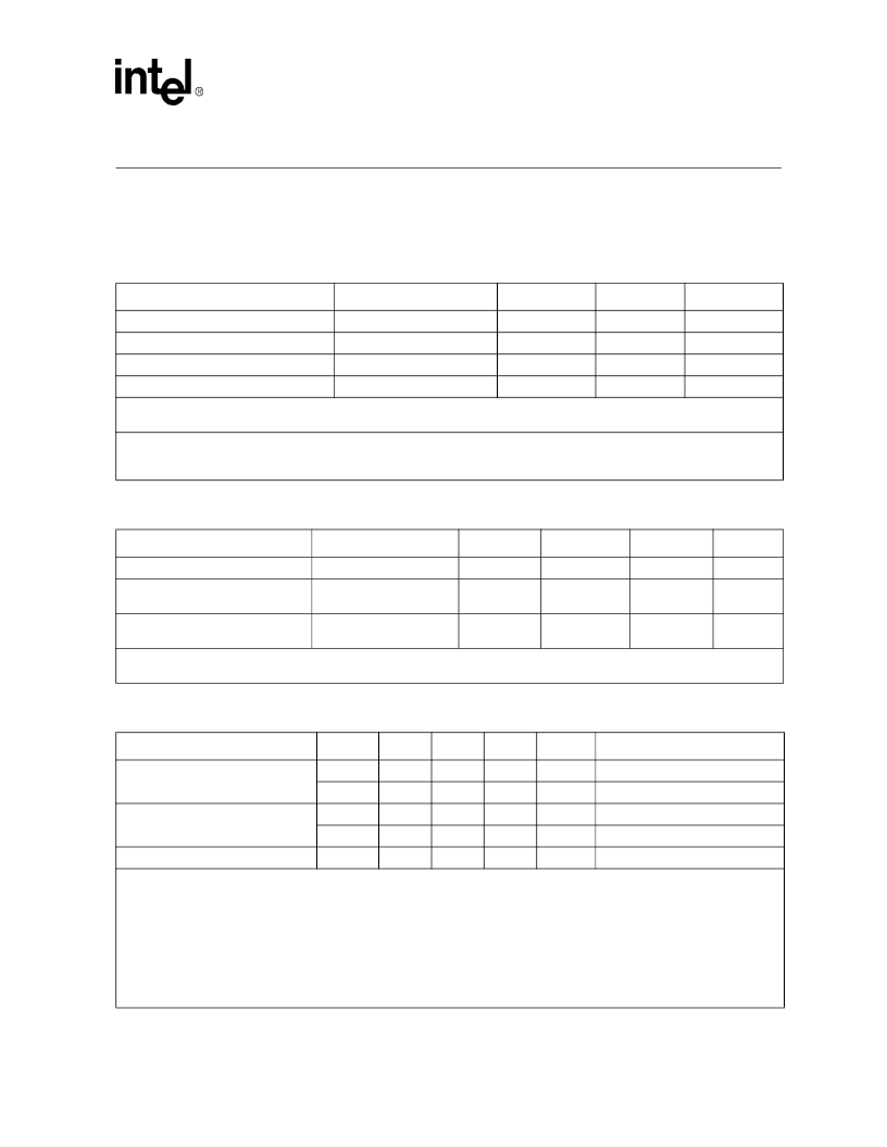
Table 8. Absolute Maximum Ratings
Parameter
Sym
Min
Max
Unit
DC supply (referenced to GND)
VCC, TVCC0, TVCC1
-0.3
6.0
V
Input voltage, any pin
1
V
IN
GND - 0.3
Vcc + 0.3
V
Input current, any pin
2
I
IN
-10
10
mA
Storage temperature
T
ST
-65
150
°
C
Caution:
Operations at or beyond these limits may result in permanent damage to the device.
Normal operation is not guaranteed or implied at these extremes.
1. Excluding RTIP and RRING which must stay within - 6 V to VCC + 0.3 V.
2. Transient currents of up to 100 mA will not cause SCR latch-up. TTIP0 & 1, TRING0 & 1, VCC, TVCC0 & 1 and TGND0 & 1
can withstand continuous current of 100 mA.
Table 9. Recommended Operating Conditions
Parameter
Symbol
Minimum
Typical
1
Maximum
Unit
DC supply
2
VCC, TVCC0, TVCC1
4.75
5.0
5.25
V
LXT331PE & QE
ambient
operating temperature
T
A
-40
25
85
°
C
LXT331PH & QH
ambient
operating temperature
T
A
-5
25
85
°
C
1. Typical figures are at 25
°
C and are for design aid only; not guaranteed and not subject to production testing.
2. Variation between TVCC0, TVCC1 and VCC must be less than 0.3 V.
Table 10. Electrical Characteristics
(Over Recommended Operating Range)
Parameter
Sym
Min
Typ
1
Max
Unit
Test Conditions
Total power dissipation - T1
2
(Maximum line length, 75
load)
PP
-
550
680
mW
-40 to +85
°
C
PD
-
550
650
mW
0 to +85
°
C
Total power dissipation - T1
3
(Maximum line length, 43
load)
PP
-
775
1000
mW
-40 to +85
°
C
PD
-
775
980
mW
0 to +85
°
C
Total power dissipation - E1
2
PD
-
380
520
mW
100% ones density
1. Typical figures are at 25
°
C and are for design aid only; not guaranteed and not subject to production testing.
2. 100% 1s density and maximum line length. Driving a line load over operating temperature range. Includes device and load.
Digital input levels are within 10% of the supply rails. Digital outputs are driving a 50 pF capacitive load.
3. 100% 1s density and maximum line length. Driving a line load (corresponding to Rt value of 9.1
and 1:2 transformer ratio)
over operating range. include device and load. Digital input levels are within 10% of the supply rails. Digital outputs are driving
a 50 pF capacitive load.
4. Functionality of pins depends on mode.
5. Output drivers will output CMOS logic levels into CMOS loads.
6. All digital input pins.
7. For MTIP0, MRING0, MTIP1 AND MRING1.
相关PDF资料 |
PDF描述 |
|---|---|
| LXT331PH | LINE INTERFACE|CMOS|LDCC|44PIN|PLASTIC |
| LXT331QE | LINE INTERFACE|CMOS|QFP|44PIN|PLASTIC |
| LXT331QH | LINE INTERFACE|CMOS|QFP|44PIN|PLASTIC |
| LXT332PE | Line Interface |
| LXT332QE | Line Interface |
相关代理商/技术参数 |
参数描述 |
|---|---|
| LXT331PH | 制造商:未知厂家 制造商全称:未知厂家 功能描述:LINE INTERFACE|CMOS|LDCC|44PIN|PLASTIC |
| LXT331QE | 制造商:未知厂家 制造商全称:未知厂家 功能描述:LINE INTERFACE|CMOS|QFP|44PIN|PLASTIC |
| LXT331QH | 制造商:未知厂家 制造商全称:未知厂家 功能描述:LINE INTERFACE|CMOS|QFP|44PIN|PLASTIC |
| LXT332 | 制造商:LVL1 制造商全称:LVL1 功能描述:Dual T1/E1 Line Interface Unit with Crystal-less Attenuation |
| LXT332PE | 制造商:未知厂家 制造商全称:未知厂家 功能描述:Line Interface |
发布紧急采购,3分钟左右您将得到回复。