- 您现在的位置:买卖IC网 > PDF目录369885 > LXT331PE LINE INTERFACE|CMOS|LDCC|44PIN|PLASTIC PDF资料下载
参数资料
| 型号: | LXT331PE |
| 英文描述: | LINE INTERFACE|CMOS|LDCC|44PIN|PLASTIC |
| 中文描述: | 线路接口|的CMOS | LDCC | 44PIN |塑料 |
| 文件页数: | 8/32页 |
| 文件大小: | 395K |
| 代理商: | LXT331PE |
第1页第2页第3页第4页第5页第6页第7页当前第8页第9页第10页第11页第12页第13页第14页第15页第16页第17页第18页第19页第20页第21页第22页第23页第24页第25页第26页第27页第28页第29页第30页第31页第32页
LXT331
—
Dual T1/E1 Line Interface Unit
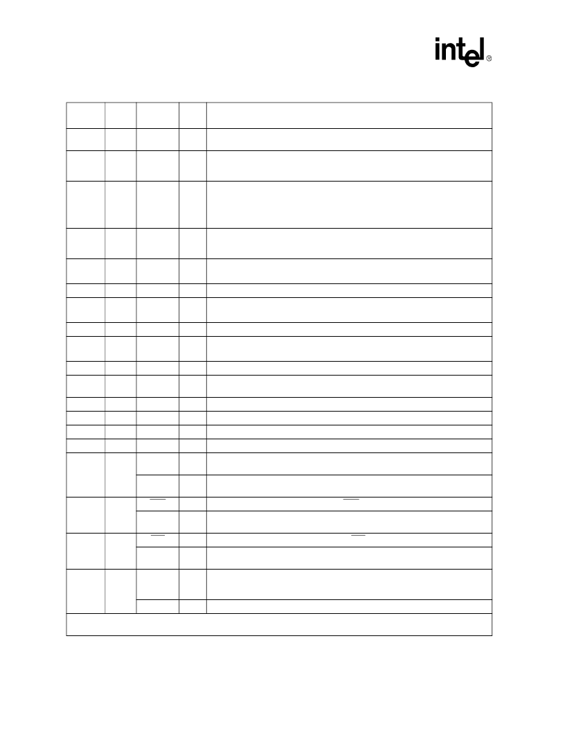
8
Datasheet
16
10
TVCC0
S
+ 5 VDC Power Supply, Port 0 Transmit Driver.
TVCC0 must not vary from TVCC1
or VCC by more than ± 0.3 V.
17
11
TRING0
AO
Transmit Ring, Port 0
. The TTIP and TRING pins are differential driver outputs
designed to drive a 35-200
load. Line matching resistors and transformers can be
selected to give the desired pulse height.
18
19
12
13
MTIP0
MRING0
AI
AI
Monitor Tip and Ring, Port 0
. These pins monitor tip and ring outputs of either its
own, or those of an adjacent LXT331 on the same board. If the application does not
use this feature, tie one of these pins to a clock source and the other to a mid-level
(referenced to the clock signal) voltage. The clock frequency can range from 100 kHz
to the TCLK frequency.
20
14
DPM0
DO
Driver Performance Monitor, Port 0
. Goes High to indicate the detection of 63
consecutive zeros. Goes Low upon the receipt of a one on the transmit monitor loop
(MTIP/MRING).
21
22
15
16
RTIP0
RRING0
AI
AI
Receive Tip and Ring, Port 0
. RTIP and RRING comprise the receive line interface.
This input pair should be connected to the line through a 1:1 transformer.
23
17
DFM0
DO
Driver Fail Monitor, Port 0
. Goes High to indicate a driver output short condition.
24
25
18
19
RRING1
RTIP1
AI
AI
Receive Tip and Ring, Port 1
. Refer to RRING0 and RTIP0 pins.
26
20
DPM1
DO
Driver Performance Monitor
,
Port 1
. Refer to DPM0 pin.
27
28
21
22
MRING1
MTIP0
AI
Monitor Tip and Ring, Port 1
. Refer to MRING0 and MTIP0 pins.
29
23
TRING1
AO
Transmit Ring, Port 1
. Refer to TRING0 pin.
30
24
TVCC1
S
+ 5 VDC Power Supply, Port 1 Transmit Driver.
TVCC1 must not deviate from
TVCC0 or VCC by more than ± 0.3 V.
31
25
TGND1
S
Ground, Port 1 Transmit Driver.
Ground return for TVCC1 power supply.
32
26
TTIP1
AO
Transmit Tip, Port 1
. Refer to TTIP0 pin.
33
27
VCC
S
+ 5 VDC Power Supply Input for All Circuits Except Transmit Drivers.
34
28
DFM1
DO
Driver Fail Monitor, Port 1
. Refer to DFM0 pin.
35
29
SPE
DI
Serial Port Enable
(Host mode)
. SPE must be clocked with MCLK, TCLK0 or
TCLK1 to enable Host mode control through the serial port.
LEN01
DI
Line Length Equalizer 0, Port 1
(Hardware mode)
.
Determines the shape and
amplitude of the transmit pulse. Refer to
Table 2 on page 12
36
30
INT1
DO
Interrupt, Port 1
(Host mode).
Refer to INT0 pin.
LEN11
DI
Line Length Equalizer 1, Port 1
(Hardware mode)
.
Determines the shape and
amplitude of the transmit pulse. Refer to
Table 2 on page 12
37
31
PS1
DI
Port Select, Port 1
(Host mode)
. Refer to PS0 pin.
LEN21
DI
Line Length Equalizer 2, Port 1
(Hardware mode)
.
Determines the shape and
amplitude of the transmit pulse. Refer to
Table 2 on page 12
38
32
SDO
DO
Serial Data Output
(Host mode)
.
Read data from the LXT331 registers are output on
this pin. When CLKE is High, SDO is valid on the rising edge of SCLK. When CLKE is
Low, SDO is valid on the falling edge of SCLK.
TAOS1
DI
Transmit All Ones Enable, Port 1
(Hardware mode)
.
Refer to TAOS0 pin.
Table 1. Pin Descriptions (Continued)
Pin
PLCC
Pin
QFP
Symbol
I/O
1
Description
1. DI = Digital Input; DO = Digital Output; DI/O = Digital Input/Output; AI = Analog Input; AO = Analog Output; S = Power
Supply
相关PDF资料 |
PDF描述 |
|---|---|
| LXT331PH | LINE INTERFACE|CMOS|LDCC|44PIN|PLASTIC |
| LXT331QE | LINE INTERFACE|CMOS|QFP|44PIN|PLASTIC |
| LXT331QH | LINE INTERFACE|CMOS|QFP|44PIN|PLASTIC |
| LXT332PE | Line Interface |
| LXT332QE | Line Interface |
相关代理商/技术参数 |
参数描述 |
|---|---|
| LXT331PH | 制造商:未知厂家 制造商全称:未知厂家 功能描述:LINE INTERFACE|CMOS|LDCC|44PIN|PLASTIC |
| LXT331QE | 制造商:未知厂家 制造商全称:未知厂家 功能描述:LINE INTERFACE|CMOS|QFP|44PIN|PLASTIC |
| LXT331QH | 制造商:未知厂家 制造商全称:未知厂家 功能描述:LINE INTERFACE|CMOS|QFP|44PIN|PLASTIC |
| LXT332 | 制造商:LVL1 制造商全称:LVL1 功能描述:Dual T1/E1 Line Interface Unit with Crystal-less Attenuation |
| LXT332PE | 制造商:未知厂家 制造商全称:未知厂家 功能描述:Line Interface |
发布紧急采购,3分钟左右您将得到回复。