- 您现在的位置:买卖IC网 > PDF目录224116 > M-986-1R2PL (CLARE INC) MFC Transceivers PDF资料下载
参数资料
| 型号: | M-986-1R2PL |
| 厂商: | CLARE INC |
| 元件分类: | 信令电路 |
| 英文描述: | MFC Transceivers |
| 中文描述: | TELECOM, MF SIGNALING CIRCUIT, PQCC44 |
| 封装: | PLASTIC, LCC-44 |
| 文件页数: | 10/13页 |
| 文件大小: | 520K |
| 代理商: | M-986-1R2PL |
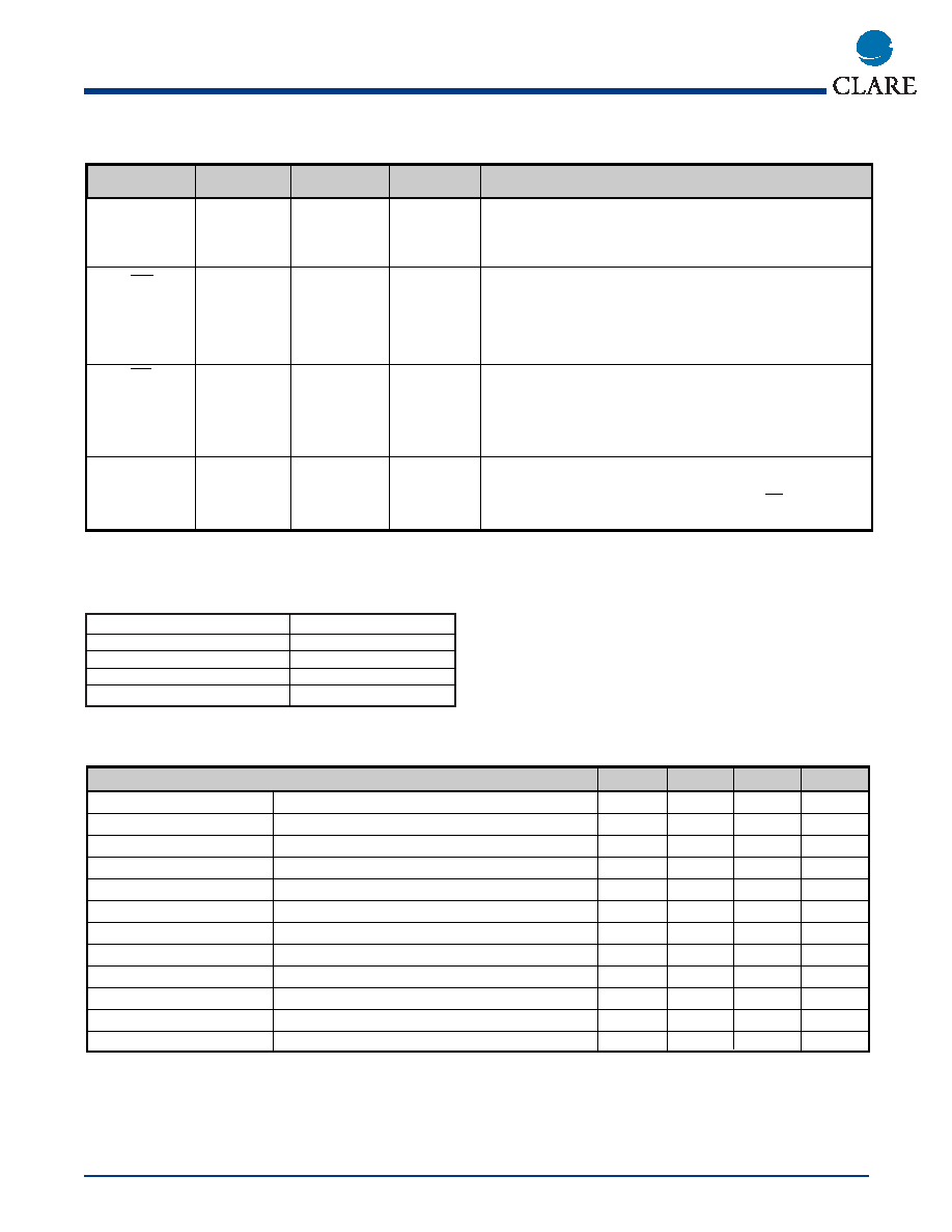
Serial Port Timing
Parameter
Min
Nom
Max
Units
t
d (CH-FR)
Internal framing delay from SCLK rising edge
-
70
ns
t
d (DX1-CL)
DX bit 1 valid before SCLK falling edge
20
-
ns
t
d (DX2-CL)
DX bit 2 valid before SCLK falling edge
20
-
ns
t
h (DX)
DX hold time after SCLK falling edge
244
-
ns
t
su (DR)
DR setup time before SCLK falling edge
20
-
ns
t
h (DR)
DR hold time after SCLK falling edge
20
-
ns
t
c (SCLK)
Serial port clock cycle time
399
488.28
4770
ns
t
f (SCLK)
Serial port clock fall time
-
30
ns
t
r (SCLK)
Serial port clock rise time
-
30
ns
t
w (SCLKL)
Serial port clock low-pulse duration*
220
244.14
2500
ns
t
w (SCLKH)
Serial port clock high-pulse duration*
220
244.14
2500
ns
t
su (FS)
FSX/FSR setup time before SCLK falling edge
100
-
ns
* The duty cycle of the serial port clock must be within 45% to 55%.
Supply voltage range, V
CC
-0.3 V to 7 V
Input voltage range
-0.3 V to 15 V
Output voltage range
-0.3 V to 15 V
Ambient air temperature range
0°C to 70°C
Storage temperature range
-45°C to 150°C
Signal Description (continued)
Signal
DIP
PLCC
I/O/Z
Description
Pinout
FR
37
41
O
8 kHz internal serial-port framing output. If internal clocking is
selected, serial-port transmit and receive operations occur
simultaneously on an active (high) FR framing pulse.
FSR
39
43
I
8 kHz external serial-port receive-framing input. If external clocking
is selected, data is received via the receive pins (DR1 and DR0) on
the active (low) FSR input. The falling edge of FSR initiates the
receive process, and the rising edge causes the M-986 to process
the data.
FSX
38
42
I
8 kHz external serial-port transmit-framing input. If external clocking
is enabled, data is transmitted on the transmit pins (DX1, DX0) on
the active (low) input. The falling edge of FSX initiates the transmit
process,and the rising edge causes the M-986 to internally load data
for the next cycle.
SCLK
34
38
I/O/Z
2.048 MHz serial-port clock. Master clock for transmitting and
receiving serial-port data. Configured as an input in external clocking
mode or output in internal clocking mode. Reset (RS) forces SCLK
to the high-impedance state.
www.clare.com
6
M-986-2R2
Rev. 3
Absolute Maximum Ratings Over Specified
Temperature
Absolute Maximum Ratings are stress ratings. Stresses in
excess of these ratings can cause permanent damage to
the device. Functional operation of the device at these or
any other conditions beyond those indicated in the opera-
tional sections of this data sheet is not implied. Exposure of
the device to the absolute maximum ratings for an extend-
ed period may degrade the device and effect its reliability.
相关PDF资料 |
PDF描述 |
|---|---|
| M-986-2R2PL | MFC Transceivers |
| M-991-01SM | Call Progress Tone Generator |
| M0736LC400 | 736 A, 4000 V, SILICON, RECTIFIER DIODE |
| M0736LC440 | 736 A, 4400 V, SILICON, RECTIFIER DIODE |
| M10BNP-332 | SHIELDED, VARIABLE INDUCTOR |
相关代理商/技术参数 |
参数描述 |
|---|---|
| M9862 | 制造商:Tamura Corporation of America 功能描述: |
| M-986-2A1 | 制造商:CLARE 制造商全称:Clare, Inc. 功能描述:MF Transceiver |
| M-986-2A1P | 功能描述:固态继电器-PCB安装 MF Transceiver, dual channel, 40xpin RoHS:否 制造商:Omron Electronics 控制电压范围: 负载电压额定值:40 V 负载电流额定值:120 mA 触点形式:1 Form A (SPST-NO) 输出设备:MOSFET 封装 / 箱体:USOP-4 安装风格:SMD/SMT |
| M-986-2A1PL | 功能描述:固态继电器-PCB安装 MF Transceiver, dual channel, 44xpin RoHS:否 制造商:Omron Electronics 控制电压范围: 负载电压额定值:40 V 负载电流额定值:120 mA 触点形式:1 Form A (SPST-NO) 输出设备:MOSFET 封装 / 箱体:USOP-4 安装风格:SMD/SMT |
| M-986-2R2 | 制造商:CLARE 制造商全称:Clare, Inc. 功能描述:MFC Transceivers |
发布紧急采购,3分钟左右您将得到回复。