- 您现在的位置:买卖IC网 > PDF目录149418 > M1010-01-155.5200 (INTEGRATED DEVICE TECHNOLOGY INC) PLL BASED CLOCK DRIVER, 1 TRUE OUTPUT(S), 0 INVERTED OUTPUT(S), CQCC36 PDF资料下载
参数资料
| 型号: | M1010-01-155.5200 |
| 厂商: | INTEGRATED DEVICE TECHNOLOGY INC |
| 元件分类: | 时钟及定时 |
| 英文描述: | PLL BASED CLOCK DRIVER, 1 TRUE OUTPUT(S), 0 INVERTED OUTPUT(S), CQCC36 |
| 封装: | 9 X 9 MM, CERAMIC, LCC-36 |
| 文件页数: | 2/8页 |
| 文件大小: | 154K |
| 代理商: | M1010-01-155.5200 |
M1010-01 Datasheet Rev 0.5
2 of 8
Revised 30Mar2005
Integr ate d Circuit Systems , In c. ● Comm unication s Modules ● www.icst.com ● tel (508) 852-5400
Integrated
Circuit
Systems, Inc.
M1010-01
VCSO BASED CLOCK JITTER ATTENUATOR
Preliminar y In f o r m atio n
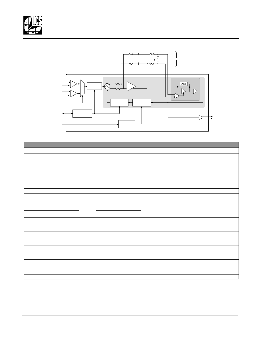
DETAILED BLOCK DIAGRAM
Figure 3: Detailed Block Diagram
PIN DESCRIPTIONS
Number
Name
I/O
Configuration
Description
1, 2, 3, 10, 14, 26
GND
Ground
Power supply ground connections.
4
9
OP_IN
nOP_IN
Input
External loop filter connections.
See Figure 4, External Loop Filter, on pg. 4.
5
8
nOP_OUT
OP_OUT
Output
6
7
nVC
VC
Input
11, 18, 19, 33
VCC
Power
Power supply connection, connect to +3.3V.
12, 13, 17, 25, 32
NC
No internal connection.
15
16
FOUT
nFOUT
Output
No internal terminator
Clock output pairs. Differential LVPECL.
20
nDIF_REF1
Input
Internal pull-UP resistor1
Note 1: For typical values of internal pull-down and pull-up resistors, see “Inputs with Pull-down” and “Inputs with Pull-up”
in Table 8, DC Characteristics, on pg. 6.
Reference clock input pair.
Differential LVPECL or LVDS.
21
DIF_REF1
Internal pull-down resistor1
22
REF_SEL
Input
Internal pull-down resistor1
Reference clock input selection. LVCMOS/LVTTL:
Logic 1 selects DIF_REF1, nDIF_REF1.
Logic 0 selects DIF_REF0, nDIF_REF0.
23
nDIF_REF0
Input
Internal pull-UP resistor1
Reference clock input pair.
Differential LVPECL or LVDS.
24
DIF_REF0
Internal pull-down resistor1
27
28
FIN_SEL1
FIN_SEL0
Input
Internal pull-down resistor1
I
nput clock frequency selection. LVCMOS/LVTTL.
See Table 3, Mfin (Frequency Input) Divider Look-Up Table
(LUT) on pg. 3.
29
30
31
SEL0
SEL1
SEL2
Input
Internal pull-UP resistor1
M and R divider value selection. LVCMOS/ LVTTL.
See Table 4, SEL2:0 Look-up Table (LUT) on pg. 3.
34, 35, 36
DNC
Do Not Connect.
Table 2: Pin Descriptions
Phase
Locked
Loop
(PLL)
M1010
SAW Delay Line
Phase
Shifter
VCSO
C
POST
C
POST
VC
nVC
R
POST
nOP_OUT
OP_OUT
R
POST
R
LOOP
R
LOOP
C
LOOP
C
LOOP
R
IN
R
IN
OP_IN
nOP_IN
Phase
Detector
Loop Filter
Amplifier
External
Loop Filter
Components
FOUT
nFOUT
SEL2:0
FIN_SEL1:0
R Div
MUX
0
REF_SEL
DIF_REF1
nDIF_REF1
DIF_REF0
nDIF_REF0
1
2
Divider LUT
3
Mfin Divider
LUT
Mfin Divider
M Div
相关PDF资料 |
PDF描述 |
|---|---|
| M210E622.080-063K | SPECIALTY LOGIC CIRCUIT, MDIP24 |
| M210E622.080-064M | SPECIALTY LOGIC CIRCUIT, MDIP24 |
| M210E622.080-069K | SPECIALTY LOGIC CIRCUIT, MDIP24 |
| M200PXXX.XXXX-222M | SPECIALTY LOGIC CIRCUIT, MDIP24 |
| M200PXXX.XXXX-223M | SPECIALTY LOGIC CIRCUIT, MDIP24 |
相关代理商/技术参数 |
参数描述 |
|---|---|
| M1010-01-156.2500 | 制造商:ICS 制造商全称:ICS 功能描述:VCSO BASED CLOCK JITTER ATTENUATOR |
| M1010-01I155.5200 | 制造商:ICS 制造商全称:ICS 功能描述:VCSO BASED CLOCK JITTER ATTENUATOR |
| M1010-01I156.2500 | 制造商:ICS 制造商全称:ICS 功能描述:VCSO BASED CLOCK JITTER ATTENUATOR |
| M10100600 | 制造商:Nortools International Ltd 功能描述:MASONRY DRILL BIT,6MM |
| M10100800 | 制造商:Nortools International Ltd 功能描述:MASONRY DRILL BIT,8MM |
发布紧急采购,3分钟左右您将得到回复。