- 您现在的位置:买卖IC网 > PDF目录296341 > M2051-11I669.6429 (INTEGRATED DEVICE TECHNOLOGY INC) VOLTAGE CONTROLLED CLOCK SAW OSCILLATOR, 669.6429 MHz PDF资料下载
参数资料
| 型号: | M2051-11I669.6429 |
| 厂商: | INTEGRATED DEVICE TECHNOLOGY INC |
| 元件分类: | XO, clock |
| 英文描述: | VOLTAGE CONTROLLED CLOCK SAW OSCILLATOR, 669.6429 MHz |
| 封装: | LEADLESS, CERAMIC PACKAGE-36 |
| 文件页数: | 8/12页 |
| 文件大小: | 504K |
| 代理商: | M2051-11I669.6429 |
M2050/51/52 Datasheet Rev 1.0
5 of 12
Revised 23Jun2005
M2050/51/52
SAW PLL FOR 10GBE 64B/66B FEC
Preliminar y In f o r m atio n
dividers also control the phase detector frequency. The
feedback divider (labeled “Mfin Divider”) provides the
broader division options needed to accomodate various
reference clock frequencies.
For example, the M2051-11-625.0000 (see “Ordering
frequency:
enable the M2051-11-625.0000 to accept “base” input
reference frequencies of: 625.00MHz (“10GbE”),
644.5313
MHz (“10GbE LAN”), and 669.6429MHz
(“10GbE 255/238 FEC
”).
The Mfin feedback divider enables the actual input
reference clock to be the base input frequency
divided by 1, 4, 5, or 25. Therefore, for the base input
frequency of 625.00MHz, the actual input reference
clock frequencies can be: 625.00, 156.25, 125.00, and
25.00
The M2050/51/52 includes a Loss of Lock (LOL)
indicator, which provides status information to system
management software. A Narrow Bandwidth (NBW)
control pin is provided as an additional mechanism for
adjusting PLL loop bandwidth without affecting the
phase detector frequency.
Options are available for Hitless Switching (HS) with or
without Phase Build-out (PBO). Performance conforms
with SONET/ SDH MTIE and TDEV during a reference
clock reselection.
Allowance for a single-ended input has been facilitated
by a unique input resistor bias scheme, which is
described next and shown in Figure 4.
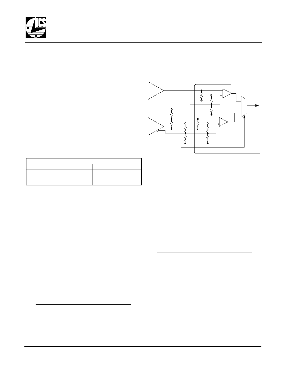
Input Reference Clocks
Two clock reference inputs and a selection mux are
provided. Either reference clock input can accept a
differential clock signal (such as LVPECL or LVDS) or
a single-ended clock input (LVCMOS or LVTTL on the
non-inverting input).
A single-ended reference clock on the unselected
reference input can cause an increase in output
clock jitter. For this reason, differential reference
inputs are preferred; interference from a differential
input on the non-selected input is minimal.
Configuration of single-ended input has been facilitated
by biasing nDIF_REF0 and nDEF_REF1 to Vcc/2, with 50k
to Vcc and 50k
to ground. The input clock structure,
and how it is used with either LVCMOS/LVTTL inputs or
a DC- coupled LVPECL clock, is shown in Figure 4.
Figure 4: Input Reference Clocks
Differential Inputs
Differential LVPECL inputs are connected to both
reference input pins in the usual manner. The external
load termination resistors shown in Figure 4 (the 127
and 82
resistors) is ideally suited for both AC and DC
coupled LVPECL reference clock lines. These provide
the 50
load termination and the VTT bias voltage.
Single-ended Inputs
Single-ended inputs (LVCMOS or LVTTL) are
connected to the non-inverting reference input pin
(DIF_REF0 or DIF_REF1). The inverting reference input pin
(nDIF_REF0 or nDIF_REF1) must be left unconnected.
In single-ended operation, when the unused inverting
input pin (nDIF_REF0 or nDEF_REF1) is left floating (not
connected), the input will self-bias at VCC/2.
PLL Operation
The M2050/51/52 is a complete clock PLL. It uses a
phase detector and configurable dividers to
synchronize the output of the VCSO with the selected
reference clock.
The PLL will work correctly, meaning it will phase-lock
the VCSO output to the input reference clock, when the
internal phase detector inputs are able to run at the
same frequency. This means the PLL dividers must be
set appropriately and a suitable reference frequency
must be chosen for the intended output frequency.
When the PLL is not set up appropriately, the VCSO is
Key to Device Variants and Look-up Table Options
Device
Variant
Look-up Table Option
Mfin Lookup Table is:
Mfec Look-up Table is:
M2050
Table 3
Table 4 (mapper LUT)
M2051
Table 5 (de-mapper LUT)
M2052
Table 6 (de-mapper LUT)
MUX
0
REF_SEL
1
VCC
50k
VCC
50k
LVCMOS/
LVTTL
LVPECL
50k
VCC
82
127
VCC
82
127
X
相关PDF资料 |
PDF描述 |
|---|---|
| M2052-11-670.8386 | VOLTAGE CONTROLLED CLOCK SAW OSCILLATOR, 670.8386 MHz |
| M2050-11I666.5143 | VOLTAGE CONTROLLED CLOCK SAW OSCILLATOR, 666.5143 MHz |
| M2052-11I669.3266 | VOLTAGE CONTROLLED CLOCK SAW OSCILLATOR, 669.3266 MHz |
| M2052-12I669.1281 | VOLTAGE CONTROLLED CLOCK SAW OSCILLATOR, 669.1281 MHz |
| M2050-13-669.3120 | VOLTAGE CONTROLLED CLOCK SAW OSCILLATOR, 669.312 MHz |
相关代理商/技术参数 |
参数描述 |
|---|---|
| M2052 | 制造商:ICS 制造商全称:ICS 功能描述:SAW PLL FOR 10GBE 64B/66B FEC |
| M2052-11-625.0000 | 制造商:ICS 制造商全称:ICS 功能描述:SAW PLL FOR 10GBE 64B/66B FEC |
| M2052-11I625.0000 | 制造商:ICS 制造商全称:ICS 功能描述:SAW PLL FOR 10GBE 64B/66B FEC |
| M2053-11-644.5313 | 功能描述:时钟合成器/抖动清除器 FREQUENCY TRANSLATOR RoHS:否 制造商:Skyworks Solutions, Inc. 输出端数量: 输出电平: 最大输出频率: 输入电平: 最大输入频率:6.1 GHz 电源电压-最大:3.3 V 电源电压-最小:2.7 V 封装 / 箱体:TSSOP-28 封装:Reel |
| M2053-11-644.5313T | 功能描述:时钟合成器/抖动清除器 FREQUENCY TRANSLATOR RoHS:否 制造商:Skyworks Solutions, Inc. 输出端数量: 输出电平: 最大输出频率: 输入电平: 最大输入频率:6.1 GHz 电源电压-最大:3.3 V 电源电压-最小:2.7 V 封装 / 箱体:TSSOP-28 封装:Reel |
发布紧急采购,3分钟左右您将得到回复。