- 您现在的位置:买卖IC网 > PDF目录377803 > M25PE10-VMP6TP (意法半导体) 4 Mbit Uniform Sector, Serial Flash Memory PDF资料下载
参数资料
| 型号: | M25PE10-VMP6TP |
| 厂商: | 意法半导体 |
| 元件分类: | DRAM |
| 英文描述: | 4 Mbit Uniform Sector, Serial Flash Memory |
| 中文描述: | 4兆位统一部门,串行闪存 |
| 文件页数: | 52/60页 |
| 文件大小: | 310K |
| 代理商: | M25PE10-VMP6TP |
第1页第2页第3页第4页第5页第6页第7页第8页第9页第10页第11页第12页第13页第14页第15页第16页第17页第18页第19页第20页第21页第22页第23页第24页第25页第26页第27页第28页第29页第30页第31页第32页第33页第34页第35页第36页第37页第38页第39页第40页第41页第42页第43页第44页第45页第46页第47页第48页第49页第50页第51页当前第52页第53页第54页第55页第56页第57页第58页第59页第60页
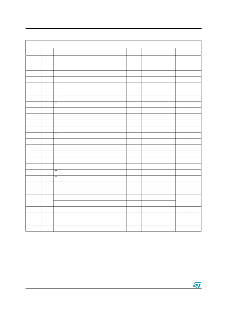
DC and AC parameters
M25PE20, M25PE10
52/60
AC characteristics (50 MHz operation,
T9HX (0.11μm) process
(1)
)
(2)
(3)
Table 22.
Test conditions specified in
Table 16
and
Table 17
Symbol
Alt.
Parameter
Min.
Typ.
Max.
Unit
f
C
f
C
Clock Frequency for the following instructions:
FAST_READ, RDLR, PW, PP, WRLR, PE, SE,
SSE, DP, RDP, WREN, WRDI, RDSR, WRSR
D.C.
50
MHz
f
R
Clock Frequency for READ instructions
D.C.
33
MHz
t
CH(4)
t
CL(4)
t
CLH
t
CLL
Clock High Time
9
ns
Clock Low Time
Clock Slew Rate
2
(peak to peak)
S Active Setup Time (relative to C)
9
ns
0.1
V/ns
t
SLCH
t
CHSL
t
DVCH
t
CHDX
t
CHSH
t
SHCH
t
SHSL
t
SHQZ(5)
t
CLQV
t
CLQX
t
WHSL(6)
t
SHWL(6)
t
DP(5)
t
RDP(5)
t
W
t
PW(7)
t
CSS
5
ns
S Not Active Hold Time (relative to C)
5
ns
t
DSU
t
DH
Data In Setup Time
2
ns
Data In Hold Time
5
ns
S Active Hold Time (relative to C)
5
ns
S Not Active Setup Time (relative to C)
5
ns
t
CSH
t
DIS
t
V
t
HO
S Deselect Time
100
ns
Output Disable Time
8
ns
Clock Low to Output Valid
8
ns
Output Hold Time
0
ns
Write Protect Setup Time
50
ns
Write Protect Hold Time
100
ns
S to Deep Power-down
3
μs
S High to Standby Mode
30
μs
Write Status Register Cycle Time
3
15
ms
Page Write Cycle Time (256 bytes)
11
23
ms
t
PP(7)
Page Program Cycle Time (256 bytes)
0.8
3
ms
Page Program Cycle Time (n bytes)
int(n/8) × 0.025
(8)
t
PE
t
SE
t
SSE
t
BE
Page Erase Cycle Time
10
20
ms
Sector Erase Cycle Time
1
5
s
SubSector Erase Cycle Time
40
150
ms
Bulk Erase Cycle Time
4.5
10
s
1.
See
Important note on page 6
.
2.
Preliminary data.
3.
Details of how to find the Technology Process in the marking are given in AN1995, see also
Section 13: Part numbering
.
4.
t
CH
+ t
CL
must be greater than or equal to 1/ f
C
Value guaranteed by characterization, not 100% tested in production.
5.
6.
Only applicable as a constraint for a WRSR instruction when SRWD is set at 1.
7.
When using PP and PW instructions to update consecutive bytes, optimized timings are obtained with one sequence
including all the bytes versus several sequences of only a few bytes (1
≤
n
≤
256).
int(A) corresponds to the upper integer part of A. E.g. int(12/8) = 2, int(32/8) = 4 int(15.3) =16.
8.
相关PDF资料 |
PDF描述 |
|---|---|
| M25PE20_07 | 4 Mbit Uniform Sector, Serial Flash Memory |
| M25PE20-VMN6G | 4 Mbit Uniform Sector, Serial Flash Memory |
| M25PE20-VMN6P | 4 Mbit Uniform Sector, Serial Flash Memory |
| M25PE20-VMN6TG | 4 Mbit Uniform Sector, Serial Flash Memory |
| M25PE20-VMN6TP | 4 Mbit Uniform Sector, Serial Flash Memory |
相关代理商/技术参数 |
参数描述 |
|---|---|
| M25PE16 | 制造商:NUMONYX 制造商全称:Numonyx B.V 功能描述:16-Mbit, page-erasable serial flash memory with byte-alterability, 75 MHz SPI bus, standard pinout |
| M25PE16-VMP6G | 功能描述:闪存 16 Mbit Lo Vltg Page Erasable Seral 闪存 RoHS:否 制造商:ON Semiconductor 数据总线宽度:1 bit 存储类型:Flash 存储容量:2 MB 结构:256 K x 8 定时类型: 接口类型:SPI 访问时间: 电源电压-最大:3.6 V 电源电压-最小:2.3 V 最大工作电流:15 mA 工作温度:- 40 C to + 85 C 安装风格:SMD/SMT 封装 / 箱体: 封装:Reel |
| M25PE16-VMP6P | 制造商:NUMONYX 制造商全称:Numonyx B.V 功能描述:16-Mbit, page-erasable serial flash memory with byte-alterability, 75 MHz SPI bus, standard pinout |
| M25PE16-VMP6TG | 功能描述:闪存 16 Mbit Lo Vltg Page Erasable Seral 闪存 RoHS:否 制造商:ON Semiconductor 数据总线宽度:1 bit 存储类型:Flash 存储容量:2 MB 结构:256 K x 8 定时类型: 接口类型:SPI 访问时间: 电源电压-最大:3.6 V 电源电压-最小:2.3 V 最大工作电流:15 mA 工作温度:- 40 C to + 85 C 安装风格:SMD/SMT 封装 / 箱体: 封装:Reel |
| M25PE16-VMP6TP | 制造商:NUMONYX 制造商全称:Numonyx B.V 功能描述:16-Mbit, page-erasable serial flash memory with byte-alterability, 75 MHz SPI bus, standard pinout |
发布紧急采购,3分钟左右您将得到回复。