- 您现在的位置:买卖IC网 > PDF目录359010 > M28F101-70XN1 (意法半导体) 1 Mb 128K x 8, Chip Erase FLASH MEMORY PDF资料下载
参数资料
| 型号: | M28F101-70XN1 |
| 厂商: | 意法半导体 |
| 英文描述: | 1 Mb 128K x 8, Chip Erase FLASH MEMORY |
| 中文描述: | 1 MB的128K的× 8,芯片擦除闪存 |
| 文件页数: | 5/23页 |
| 文件大小: | 197K |
| 代理商: | M28F101-70XN1 |
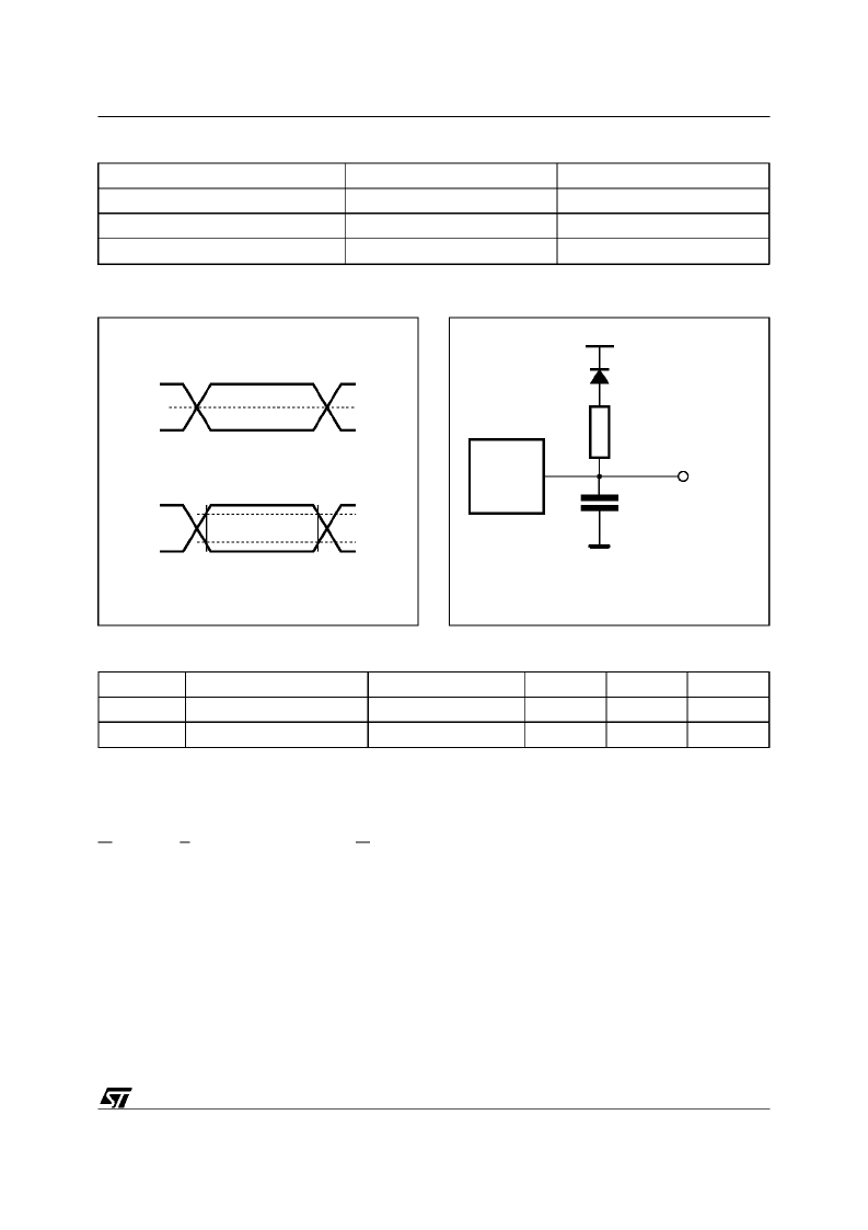
AI01275
3V
SRAM Interface
0V
1.5V
2.4V
EPROM Interface
0.45V
2.0V
0.8V
Figure 3. AC TestingInput Output Waveform
AI01276
1.3V
OUT
CL= 30pF or 100pF
CL= 30pF for SRAM Interface
CL= 100pF for EPROM Interface
CLincludes JIG capacitance
3.3k
1N914
DEVICE
UNDER
TEST
Figure 4. ACTesting Load Circuit
SRAM Interface Levels
EPROM Interface Levels
Input Rise and Fall Times
≤
10ns
≤
10ns
Input Pulse Voltages
0 to 3V
0.45V to 2.4V
Input and Output Timing Ref. Voltages
1.5V
0.8V and 2V
Table 6. AC MeasurementConditions
Symbol
Parameter
Test Condition
Min
Max
Unit
C
IN
Input Capacitance
V
IN
= 0V
6
pF
C
OUT
Output Capacitance
V
OUT
= 0V
12
pF
Note:
1. Sampled only, not 100% test.ed
Table 7. Capacitance
(1)
(T
A
= 25
°
C, f = 1 MHz )
Awriteto thecommandregisterismadebybringing
WLowwhileEisLow.ThefallingedgeofWlatches
Addresses, while the rising edge latches Data,
which are used for those commands that require
address inputs, command input or provide data
output.
The supply voltage V
CC
and the program voltage
V
PP
can be applied in any order. When the device
is powered up or when V
PP
is
≤
6.5V the contents
of the command register defaults to 00h, thus
automaticallysetting-upRead operations.In addi-
tion a specific command may be used to set the
command register to 00h for reading the memory.
The system designer may chose to provide a con-
stanthigh V
PP
and use the register commands for
all operations,or to switch the V
PP
fromlow to high
only when needing to eraseor program the mem-
ory. Allcommand register access isinhibited when
V
CC
falls below the Erase/Write Lockout Voltage
(V
LKO
) of 2.5V.
If the device is deselected during Erasure, Pro-
gramming or Verification it will draw active supply
currents until the operationsare terminated.
The device is protected against stress caused by
long erase orprogram times. If theend of Erase or
Programming operations are not terminated by a
Verify cycle within a maximum time permitted, an
internal stop timer automatically stops the opera-
tion.The deviceremains in aninactivestate, ready
to start a Verifyor ResetMode operation.
READ/WRITE MODES
(cont’d)
5/23
M28F101
相关PDF资料 |
PDF描述 |
|---|---|
| M28F101-90XN1 | 1 Mb 128K x 8, Chip Erase FLASH MEMORY |
| M28F101-100XN1 | 1 Mb 128K x 8, Chip Erase FLASH MEMORY |
| M28F101-120XN1 | 1 Mb 128K x 8, Chip Erase FLASH MEMORY |
| M28F101-150XN1 | 1 Mb 128K x 8, Chip Erase FLASH MEMORY |
| M28F101-90P1 | 1 Mb 128K x 8, Chip Erase FLASH MEMORY |
相关代理商/技术参数 |
参数描述 |
|---|---|
| M28F101-70XN3 | 制造商:STMICROELECTRONICS 制造商全称:STMicroelectronics 功能描述:1 Mb 128K x 8, Chip Erase FLASH MEMORY |
| M28F101-70XN6 | 制造商:STMICROELECTRONICS 制造商全称:STMicroelectronics 功能描述:1 Mb 128K x 8, Chip Erase FLASH MEMORY |
| M28F101-70XP1 | 制造商:STMICROELECTRONICS 制造商全称:STMicroelectronics 功能描述:1 Mb 128K x 8, Chip Erase FLASH MEMORY |
| M28F101-70XP3 | 制造商:STMICROELECTRONICS 制造商全称:STMicroelectronics 功能描述:1 Mb 128K x 8, Chip Erase FLASH MEMORY |
| M28F101-70XP6 | 制造商:STMICROELECTRONICS 制造商全称:STMicroelectronics 功能描述:1 Mb 128K x 8, Chip Erase FLASH MEMORY |
发布紧急采购,3分钟左右您将得到回复。