- 您现在的位置:买卖IC网 > PDF目录377808 > M28LV16 (意法半导体) 16K (2K x 8) Parallel EEPROM with Software Data Protection(16K低压并行EEPROM,软件数据保护) PDF资料下载
参数资料
| 型号: | M28LV16 |
| 厂商: | 意法半导体 |
| 元件分类: | DRAM |
| 英文描述: | 16K (2K x 8) Parallel EEPROM with Software Data Protection(16K低压并行EEPROM,软件数据保护) |
| 中文描述: | 16K的(2K × 8)与软件数据保护(16K的低压并行的EEPROM,软件数据保护并行的EEPROM) |
| 文件页数: | 4/17页 |
| 文件大小: | 123K |
| 代理商: | M28LV16 |
AI01520
ADDRESS
LATCH
A6-A10
(Page Address)
X
CONTROL LOGIC
64K ARRAY
ADDRESS
LATCH
A0-A5
Y DECODE
VPPGEN
RESET
SENSE AND DATA LATCH
I/O BUFFERS
E
G
W
PAGE
LOAD
TIMER
STATUS
TOGGLE BIT
DATA POLLING
DQ0-DQ7
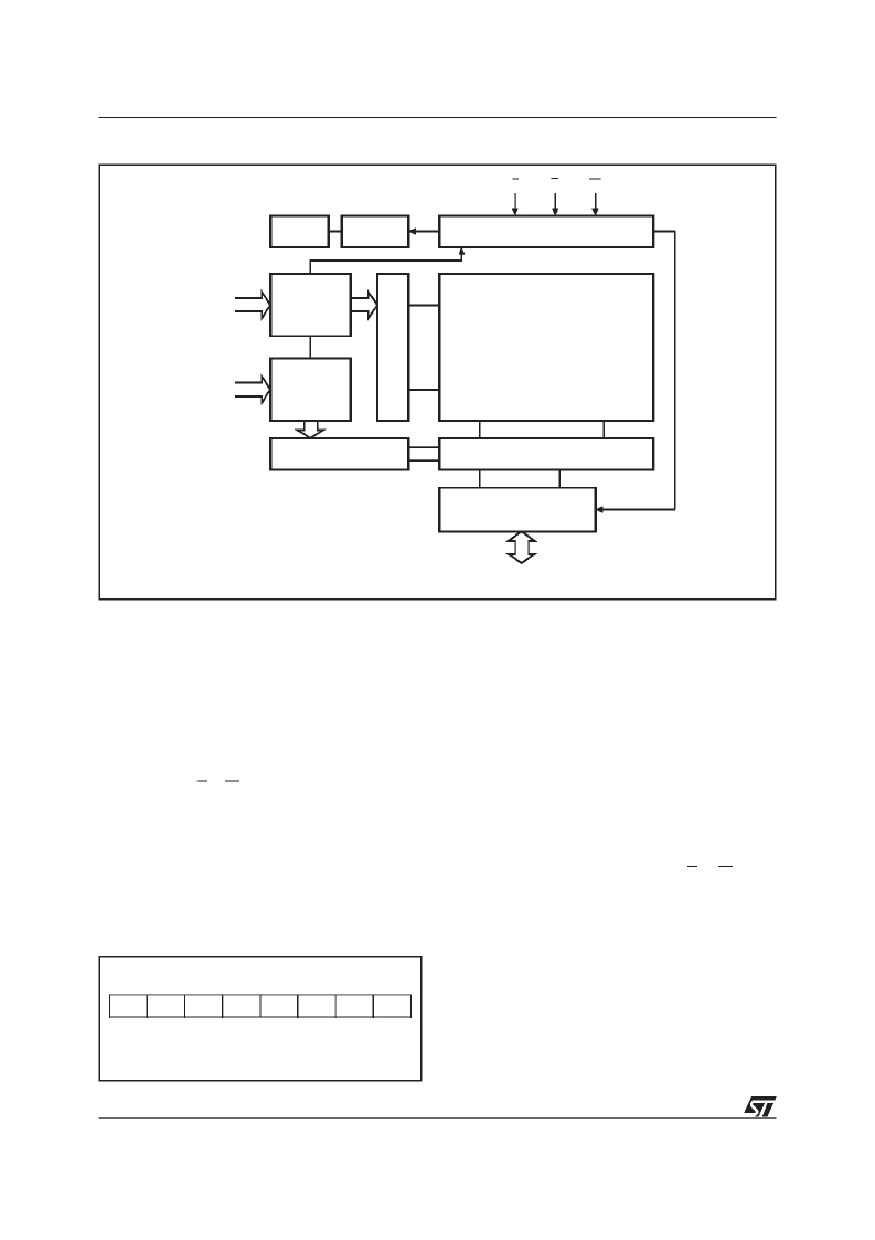
Figure3. BlockDiagram
Page Write
Page write allows up to 64 bytes to be consecu-
tively latched into the memory prior to initiating a
programming cycle.All bytes must be located in a
single page address, that is A6-A10 must be the
samefor all bytes. The page write can be initiated
during any byte write operation.
Following the first byte write instruction the host
may send another address and data with a mini-
mum datatransfer rateof 1/t
WHWH
(seeFigure13).
If atransitionofEorWisnotdetectedwithint
WHWH
,
the internalprogrammingcycle will start.
MicrocontrollerControl Interface
The M28LV16 provides two write operation status
bitsandonestatuspinthatcanbeusedtominimize
the system writecycle. Thesesignals areavailable
on the I/O port bits DQ7 or DQ6 of the memory
during programmingcycle only.
DQ7
DQ6
DQ5
DQ4
DQ3
DQ2
DQ1
DQ0
DP
TB
PLTS Hi-Z
Hi-Z
Hi-Z
Hi-Z
Hi-Z
Figure4. StatusBit Assignment
DP = Data Polling
TB = ToggleBit
PLTS = PageLoad Timer Status
Data Polling bit (DQ7).
During the internal write
cycle, any attempt to read thelast byte written will
produce on DQ7 the complementary value of the
previously latched bit. Once the write cycle is fin-
ished the true logic value appears on DQ7 in the
read cycle.
Toggle bit (DQ6).
The M28LV16 offers another
way for determiningwhen the internal write cycle
iscompleted.During the internalErase/Writecycle,
DQ6 will toggle from ”0” to ”1” and ”1” to ”0” (the
first read value is ”0”) on subsequent attempts to
read thememory. When the internalcycle is com-
pleted the toggling will stop and the device will be
accessible for a newRead or Write operation.
Page Load Timer Status bit (DQ5)
. In the Page
Write mode data may be latchedby E or W. Up to
32 bytes may be input. The Data output (DQ5)
indicates the status of the internal Page Load
Timer. DQ5 may be read by asserting Output En-
able Low (t
PLTS
). DQ5 Low indicates the timer is
running, High indicates time-out after which the
writecycle will start andno new data may be input.
4/17
M28LV16
相关PDF资料 |
PDF描述 |
|---|---|
| M28LV17 | 16K (2K x 8) Parallel EEPROM with Software Data Protection(16K低压并行EEPROM,软件数据保护) |
| M28W160B | 16 Mbit (1Mb x16, Boot Block) 3V Supply Flash Memory |
| M28W160BB1006T | 16 Mbit (1Mb x16, Boot Block) 3V Supply Flash Memory |
| M28W160BB100GBT | 16 Mbit (1Mb x16, Boot Block) 3V Supply Flash Memory |
| M28W160BB100-NT | 16 Mbit (1Mb x16, Boot Block) 3V Supply Flash Memory |
相关代理商/技术参数 |
参数描述 |
|---|---|
| M28LV64 | 制造商:STMICROELECTRONICS 制造商全称:STMicroelectronics 功能描述:64K 8K x 8 LOW VOLTAGE PARALLEL EEPROM with SOFTWARE DATA PROTECTION |
| M28LV64-200K1 | 制造商:STMICROELECTRONICS 制造商全称:STMicroelectronics 功能描述:64K 8K x 8 LOW VOLTAGE PARALLEL EEPROM with SOFTWARE DATA PROTECTION |
| M28LV64-200K6 | 制造商:STMICROELECTRONICS 制造商全称:STMicroelectronics 功能描述:64K 8K x 8 LOW VOLTAGE PARALLEL EEPROM with SOFTWARE DATA PROTECTION |
| M28LV64-200MS1 | 制造商:STMICROELECTRONICS 制造商全称:STMicroelectronics 功能描述:64K 8K x 8 LOW VOLTAGE PARALLEL EEPROM with SOFTWARE DATA PROTECTION |
| M28LV64-200MS6 | 制造商:STMICROELECTRONICS 制造商全称:STMicroelectronics 功能描述:64K 8K x 8 LOW VOLTAGE PARALLEL EEPROM with SOFTWARE DATA PROTECTION |
发布紧急采购,3分钟左右您将得到回复。