- 您现在的位置:买卖IC网 > PDF目录359024 > M29DW640D90ZA6F (意法半导体) Dual JFET-Input High-Output-Drive uPower Operational Amplifier 8-SOIC PDF资料下载
参数资料
| 型号: | M29DW640D90ZA6F |
| 厂商: | 意法半导体 |
| 英文描述: | Dual JFET-Input High-Output-Drive uPower Operational Amplifier 8-SOIC |
| 中文描述: | 64兆位(8兆x8或4Mb的x16插槽,多行,页,引导块)3V电源快闪记忆体 |
| 文件页数: | 6/56页 |
| 文件大小: | 942K |
| 代理商: | M29DW640D90ZA6F |
第1页第2页第3页第4页第5页当前第6页第7页第8页第9页第10页第11页第12页第13页第14页第15页第16页第17页第18页第19页第20页第21页第22页第23页第24页第25页第26页第27页第28页第29页第30页第31页第32页第33页第34页第35页第36页第37页第38页第39页第40页第41页第42页第43页第44页第45页第46页第47页第48页第49页第50页第51页第52页第53页第54页第55页第56页
M29DW640D
6/56
SUMMARY DESCRIPTION
The M29DW640D is a 64 Mbit (8Mb x8 or 4Mb
x16) non-volatile memory that can be read, erased
and reprogrammed. These operations can be per-
formed using a single low voltage (2.7 to 3.6V)
supply. On power-up the memory defaults to its
Read mode.
The device features an asymmetrical block archi-
tecture, with 16 parameter and 126 main blocks,
divided into four Banks, A, B, C and D, providing
multiple Bank operations. While programming or
erasing is underway in one group of banks (from 1
to 3), reading can be conducted in any of the other
banks. The bank architecture is summarized in Ta-
ble
2
. Eight of the Parameter Blocks are at the top
of the memory address space, and eight are at the
bottom.
The M29DW640D has one extra 256 Byte block
(Extended Block) that can be accessed using a
dedicated command. The Extended Block can be
protected and so is useful for storing security infor-
mation. However the protection is irreversible,
once protected the protection cannot be undone.
Each block can be erased independently, so it is
possible to preserve valid data while old data is
erased. The blocks can be protected to prevent
accidental Program or Erase commands from
modifying the memory. Program and Erase com-
mands are written to the Command Interface of
the memory. An on-chip Program/Erase Controller
simplifies the process of programming or erasing
the memory by taking care of all of the special op-
erations that are required to update the memory
contents. The end of a program or erase operation
can be detected and any error conditions identi-
fied. The command set required to control the
memory is consistent with JEDEC standards.
Chip Enable, Output Enable and Write Enable sig-
nals control the bus operation of the memory.
They allow simple connection to most micropro-
cessors, often without additional logic.
The memory is offered in TSOP48 (12x20mm) and
TFBGA63 (7x11mm, 0.8mm pitch) packages. The
memory is supplied with all the bits erased (set to
’1’).
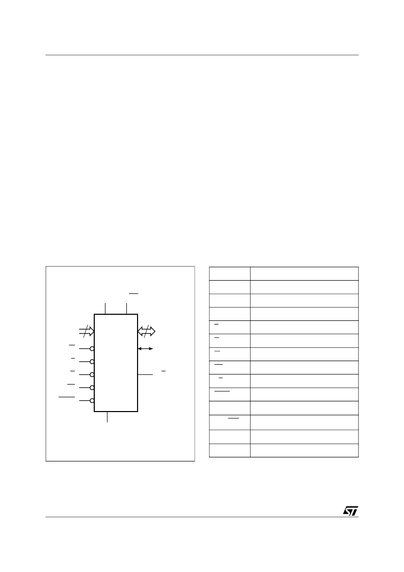
Figure 2. Logic Diagram
Table 1. Signal Names
AI06877b
22
A0-A21
W
DQ0-DQ14
VCC
M29DW640D
E
VSS
15
G
RP
DQ15A–1
RB
VPP/WP
BYTE
A0-A21
Address Inputs
DQ0-DQ7
Data Inputs/Outputs
DQ8-DQ14
Data Inputs/Outputs
DQ15A–1
Data Input/Output or Address Input
E
Chip Enable
G
Output Enable
W
Write Enable
RP
Reset/Block Temporary Unprotect
RB
Ready/Busy Output
BYTE
Byte/Word Organization Select
V
CC
Supply Voltage
V
PP
/WP
V
PP
/Write Protect
V
SS
Ground
NC
Not Connected Internally
相关PDF资料 |
PDF描述 |
|---|---|
| M29DW640D90ZA6T | Dual JFET-Input High-Output-Drive uPower Operational Amplifier 8-SOIC |
| M29DW640D90N1F | 64 Mbit (8Mb x8 or 4Mb x16, Multiple Bank, Page, Boot Block) 3V Supply Flash Memory |
| M29DW640D90N1T | 64 Mbit (8Mb x8 or 4Mb x16, Multiple Bank, Page, Boot Block) 3V Supply Flash Memory |
| M29DW640D90ZA1 | 64 Mbit (8Mb x8 or 4Mb x16, Multiple Bank, Page, Boot Block) 3V Supply Flash Memory |
| M29DW640D90N6T | 64 Mbit (8Mb x8 or 4Mb x16, Multiple Bank, Page, Boot Block) 3V Supply Flash Memory |
相关代理商/技术参数 |
参数描述 |
|---|---|
| M29DW640D90ZA6T | 制造商:STMICROELECTRONICS 制造商全称:STMicroelectronics 功能描述:64 Mbit (8Mb x8 or 4Mb x16, Multiple Bank, Page, Boot Block) 3V Supply Flash Memory |
| M29DW640F | 制造商:NUMONYX 制造商全称:Numonyx B.V 功能描述:64 Mbit (8Mb x8 or 4Mb x16, Multiple Bank, Page, Boot Block) 3V Supply Flash Memory |
| M29DW640F70N1 | 制造商:NUMONYX 制造商全称:Numonyx B.V 功能描述:64 Mbit (8Mb x8 or 4Mb x16, Multiple Bank, Page, Boot Block) 3V Supply Flash Memory |
| M29DW640F70N1E | 制造商:NUMONYX 制造商全称:Numonyx B.V 功能描述:64 Mbit (8Mb x8 or 4Mb x16, Multiple Bank, Page, Boot Block) 3V Supply Flash Memory |
| M29DW640F70N1F | 制造商:NUMONYX 制造商全称:Numonyx B.V 功能描述:64 Mbit (8Mb x8 or 4Mb x16, Multiple Bank, Page, Boot Block) 3V Supply Flash Memory |
发布紧急采购,3分钟左右您将得到回复。