- 您现在的位置:买卖IC网 > PDF目录296348 > M29F800DB70N3F (NUMONYX) 512K X 16 FLASH 5V PROM, 70 ns, PDSO48 PDF资料下载
参数资料
| 型号: | M29F800DB70N3F |
| 厂商: | NUMONYX |
| 元件分类: | PROM |
| 英文描述: | 512K X 16 FLASH 5V PROM, 70 ns, PDSO48 |
| 封装: | 12 X 20 MM, LEAD FREE, PLASTIC, TSOP-48 |
| 文件页数: | 3/39页 |
| 文件大小: | 622K |
| 代理商: | M29F800DB70N3F |
第1页第2页当前第3页第4页第5页第6页第7页第8页第9页第10页第11页第12页第13页第14页第15页第16页第17页第18页第19页第20页第21页第22页第23页第24页第25页第26页第27页第28页第29页第30页第31页第32页第33页第34页第35页第36页第37页第38页第39页
11/39
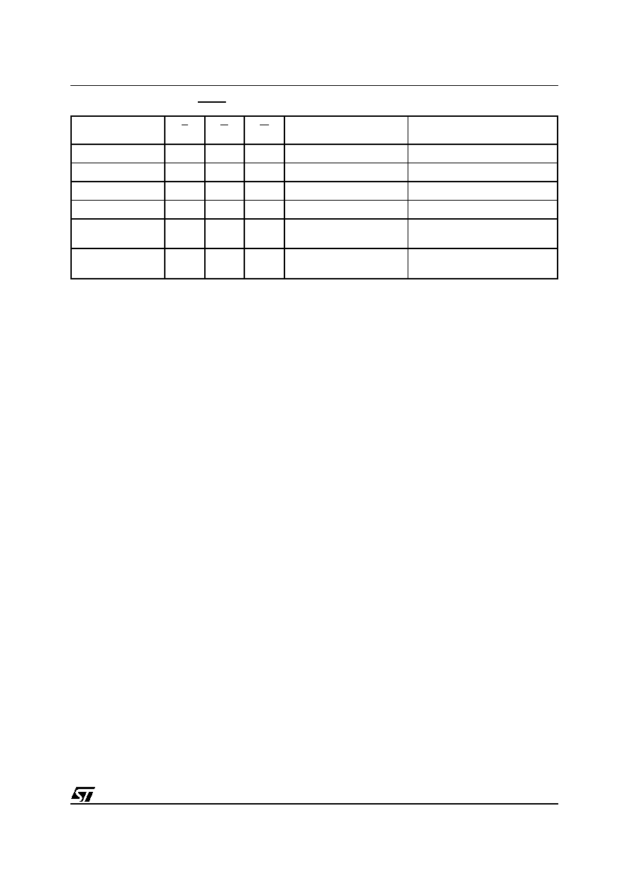
Table 3. Bus Operations, BYTE = VIH
Note: X = VIL or VIH.
COMMAND INTERFACE
All Bus Write operations to the memory are inter-
preted by the Command Interface. Commands
consist of one or more sequential Bus Write oper-
ations. Failure to observe a valid sequence of Bus
Write operations will result in the memory return-
ing to Read mode. The long command sequences
are imposed to maximize data security.
The address used for the commands changes de-
pending on whether the memory is in 16-bit or 8-
the configuration that is being used, for a summary
of the commands.
Read/Reset Command. The Read/Reset com-
mand returns the memory to its Read mode where
it behaves like a ROM or EPROM, unless other-
wise stated. It also resets the errors in the Status
Register. Either one or three Bus Write operations
can be used to issue the Read/Reset command.
The Read/Reset Command can be issued, be-
tween Bus Write cycles before the start of a pro-
gram or erase operation, to return the device to
read mode. Once the program or erase operation
has started the Read/Reset command is no longer
accepted. The Read/Reset command will not
abort an Erase operation when issued while in
Erase Suspend.
Auto Select Command. The Auto Select com-
mand is used to read the Manufacturer Code, the
Device Code and the Block Protection Status.
Three consecutive Bus Write operations are re-
quired to issue the Auto Select command. Once
the Auto Select command is issued the memory
remains in Auto Select mode until a Read/Reset
command is issued. Read CFI Query and Read/
Reset commands are accepted in Auto Select
mode, all other commands are ignored.
From the Auto Select mode the Manufacturer
Code can be read using a Bus Read operation
with A0 = VIL and A1 = VIL. The other address bits
may be set to either VIL or VIH. The Manufacturer
Code for STMicroelectronics is 0020h.
The Device Code can be read using a Bus Read
operation with A0 = VIH and A1 = VIL. The other
address bits may be set to either VIL or VIH.
The Block Protection Status of each block can be
read using a Bus Read operation with A0 = VIL,
A1 = VIH, and A12-A18 specifying the address of
the block. The other address bits may be set to ei-
ther VIL or VIH. If the addressed block is protected
then 01h is output on Data Inputs/Outputs DQ0-
DQ7, otherwise 00h is output.
Program Command. The
Program
command
can be used to program a value to one address in
the memory array at a time. The command re-
quires four Bus Write operations, the final write op-
eration latches the address and data in the internal
state machine and starts the Program/Erase Con-
troller.
If the address falls in a protected block then the
Program command is ignored, the data remains
unchanged. The Status Register is never read and
no error condition is given.
During the program operation the memory will ig-
nore all commands. It is not possible to issue any
command to abort or pause the operation. Typical
program times are given in Table 6. Bus Read op-
erations during the program operation will output
the Status Register on the Data Inputs/Outputs.
See the section on the Status Register for more
details.
After the program operation has completed the
memory will return to the Read mode, unless an
error has occurred. When an error occurs the
Operation
E
G
W
Address Inputs
A0-A18
Data Inputs/Outputs
DQ15A–1, DQ14-DQ0
Bus Read
VIL
VIH
Cell Address
Data Output
Bus Write
VIL
VIH
VIL
Command Address
Data Input
Output Disable
X
VIH
X
Hi-Z
Standby
VIH
X
Hi-Z
Read Manufacturer
Code
VIL
VIH
A0 = VIL, A1 = VIL, A9 = VID,
Others VIL or VIH
0020h
Read Device Code
VIL
VIH
A0 = VIH, A1 = VIL, A9 = VID,
Others VIL or VIH
22ECh (M29F800DT)
2258h (M29F800DB)
相关PDF资料 |
PDF描述 |
|---|---|
| M29F800DB90N6T | 512K X 16 FLASH 5V PROM, 70 ns, PDSO48 |
| M29W160BT90ZA6 | 1M X 16 FLASH 2.7V PROM, 90 ns, PBGA48 |
| M29W400BT70M6T | 256K X 16 FLASH 2.7V PROM, 70 ns, PDSO44 |
| M29W640GB70ZA6F | 4M X 16 FLASH 3V PROM, 70 ns, PBGA48 |
| M2Y51264TU88A2G-37B | 64M X 64 DDR DRAM MODULE, 0.5 ns, DMA240 |
相关代理商/技术参数 |
参数描述 |
|---|---|
| M29F800DB70N6 | 功能描述:闪存 1Mx8 or 512Kx16 70ns RoHS:否 制造商:ON Semiconductor 数据总线宽度:1 bit 存储类型:Flash 存储容量:2 MB 结构:256 K x 8 定时类型: 接口类型:SPI 访问时间: 电源电压-最大:3.6 V 电源电压-最小:2.3 V 最大工作电流:15 mA 工作温度:- 40 C to + 85 C 安装风格:SMD/SMT 封装 / 箱体: 封装:Reel |
| M29F800DB70N6E | 功能描述:闪存 STD FLASH 8 MEG RoHS:否 制造商:ON Semiconductor 数据总线宽度:1 bit 存储类型:Flash 存储容量:2 MB 结构:256 K x 8 定时类型: 接口类型:SPI 访问时间: 电源电压-最大:3.6 V 电源电压-最小:2.3 V 最大工作电流:15 mA 工作温度:- 40 C to + 85 C 安装风格:SMD/SMT 封装 / 箱体: 封装:Reel |
| M29F800DB70N6F | 功能描述:闪存 STD FLASH 8 MEG RoHS:否 制造商:ON Semiconductor 数据总线宽度:1 bit 存储类型:Flash 存储容量:2 MB 结构:256 K x 8 定时类型: 接口类型:SPI 访问时间: 电源电压-最大:3.6 V 电源电压-最小:2.3 V 最大工作电流:15 mA 工作温度:- 40 C to + 85 C 安装风格:SMD/SMT 封装 / 箱体: 封装:Reel |
| M29F800DB70N6T | 功能描述:闪存 1Mx8 or 512Kx16 70ns RoHS:否 制造商:ON Semiconductor 数据总线宽度:1 bit 存储类型:Flash 存储容量:2 MB 结构:256 K x 8 定时类型: 接口类型:SPI 访问时间: 电源电压-最大:3.6 V 电源电压-最小:2.3 V 最大工作电流:15 mA 工作温度:- 40 C to + 85 C 安装风格:SMD/SMT 封装 / 箱体: 封装:Reel |
| M29F800DT55M1 | 功能描述:闪存 SO-44 1MX8/512KX16 RoHS:否 制造商:ON Semiconductor 数据总线宽度:1 bit 存储类型:Flash 存储容量:2 MB 结构:256 K x 8 定时类型: 接口类型:SPI 访问时间: 电源电压-最大:3.6 V 电源电压-最小:2.3 V 最大工作电流:15 mA 工作温度:- 40 C to + 85 C 安装风格:SMD/SMT 封装 / 箱体: 封装:Reel |
发布紧急采购,3分钟左右您将得到回复。