- 您现在的位置:买卖IC网 > PDF目录377821 > M29W200BT120M6 (意法半导体) 2 Mbit (256Kb x8 or 128Kb x16, Boot Block) Low Voltage Single Supply Flash Memory PDF资料下载
参数资料
| 型号: | M29W200BT120M6 |
| 厂商: | 意法半导体 |
| 英文描述: | 2 Mbit (256Kb x8 or 128Kb x16, Boot Block) Low Voltage Single Supply Flash Memory |
| 中文描述: | 2兆位(256Kb的x8或128KB的x16插槽,引导块)低电压单电源闪存 |
| 文件页数: | 11/22页 |
| 文件大小: | 175K |
| 代理商: | M29W200BT120M6 |
11/22
M29W200BT, M29W200BB
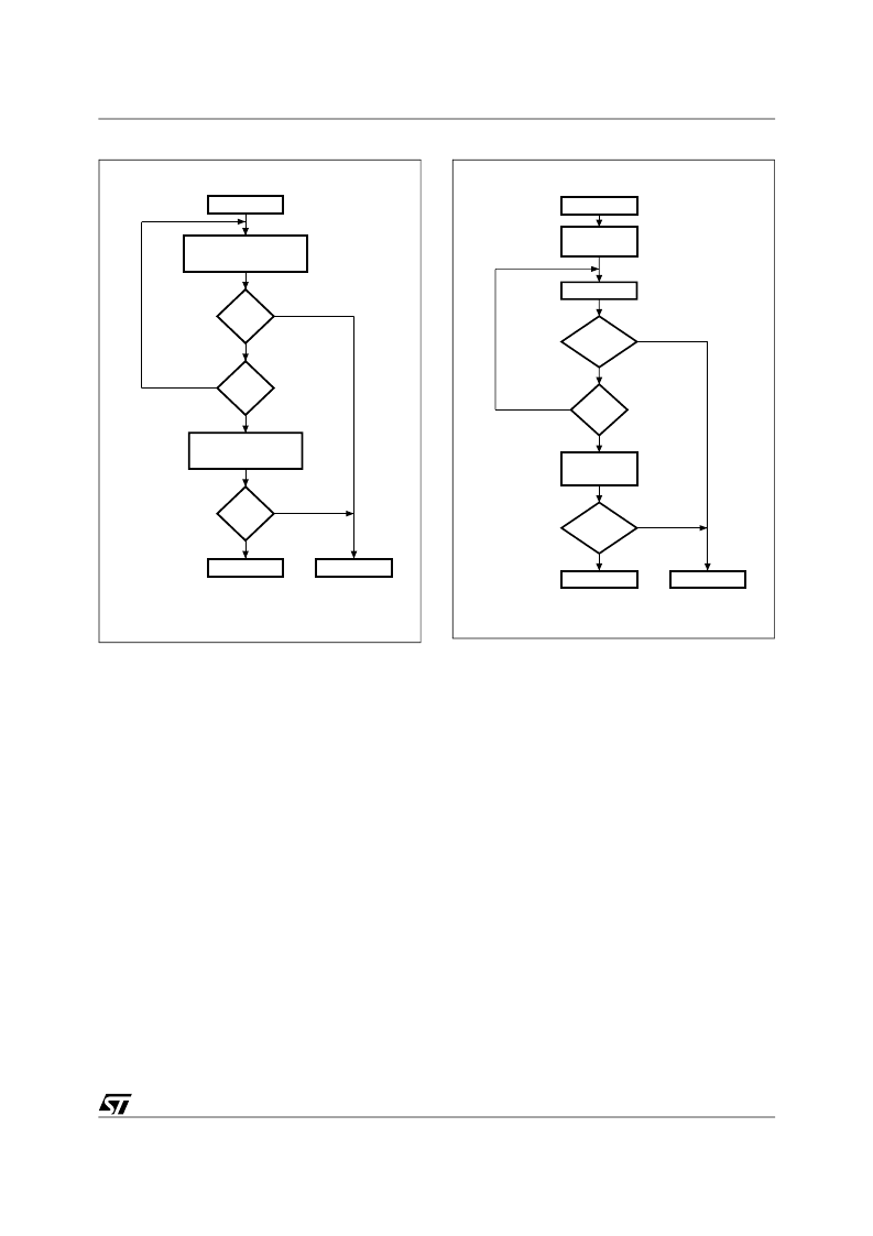
Figure 4. Data Polling Flowchart
READ DQ5 & DQ7
at VALID ADDRESS
START
READ DQ7
at VALID ADDRESS
FAIL
PASS
AI03598
D=
DATA
YES
NO
YES
NO
DQ5
= 1
D=
DATA
YES
NO
Figure 5. Data Toggle Flowchart
READ DQ6
START
READ DQ6
TWICE
FAIL
PASS
AI01370B
D=
TOGGLE
NO
NO
YES
YES
DQ5
= 1
NO
YES
D=
TOGGLE
READ
DQ5 & DQ6
Erase Timer Bit (DQ3).
The Erase Timer Bit can
be used to identify the start of Program/Erase
Controller operation during a Block Erase com-
mand. Once the Program/Erase Controller starts
erasing the Erase Timer Bit is set to ’1’. Before the
Program/Erase Controller starts the Erase Timer
Bit is set to ’0’ and additional blocks to be erased
may be written to the Command Interface. The
Erase Timer Bit is output on DQ3 when the Status
Register is read.
Alternative Toggle Bit (DQ2).
The
Toggle Bit can be used to monitor the Program/
Erase controller during Erase operations. The Al-
ternative Toggle Bit is output on DQ2 when the
Status Register is read.
During Chip Erase and Block Erase operations the
Toggle Bit changes from ’0’ to ’1’ to ’0’, etc., with
successive Bus Read operations from addresses
Alternative
within the blocks being erased. Once the operation
completes the memory returns to Read mode.
During Erase Suspend the Alternative Toggle Bit
changes from ’0’ to ’1’ to ’0’, etc. with successive
Bus Read operations from addresses within the
blocks being erased. Bus Read operations to ad-
dresses within blocks not being erased will output
the memory cell data as if in Read mode.
After an Erase operation that causes the Error Bit
to be set the Alternative Toggle Bit can be used to
identify which block or blocks have caused the er-
ror. The Alternative Toggle Bit changes from ’0’ to
’1’ to ’0’, etc. with successive Bus Read Opera-
tions from addresses within blocks that have not
erased correctly. The Alternative Toggle Bit does
not change if the addressed block has erased cor-
rectly.
相关PDF资料 |
PDF描述 |
|---|---|
| M29W200BT120M6E | 2 Mbit (256Kb x8 or 128Kb x16, Boot Block) Low Voltage Single Supply Flash Memory |
| M29W200BT120M6F | 2 Mbit (256Kb x8 or 128Kb x16, Boot Block) Low Voltage Single Supply Flash Memory |
| M29W200BT120N1 | 2 Mbit (256Kb x8 or 128Kb x16, Boot Block) Low Voltage Single Supply Flash Memory |
| M29W200BT120N1E | 2 Mbit (256Kb x8 or 128Kb x16, Boot Block) Low Voltage Single Supply Flash Memory |
| M29W200BT120N1F | 2 Mbit (256Kb x8 or 128Kb x16, Boot Block) Low Voltage Single Supply Flash Memory |
相关代理商/技术参数 |
参数描述 |
|---|---|
| M29W200BT55N1 | 功能描述:闪存 256Kx8 or 128Kx16 55 RoHS:否 制造商:ON Semiconductor 数据总线宽度:1 bit 存储类型:Flash 存储容量:2 MB 结构:256 K x 8 定时类型: 接口类型:SPI 访问时间: 电源电压-最大:3.6 V 电源电压-最小:2.3 V 最大工作电流:15 mA 工作温度:- 40 C to + 85 C 安装风格:SMD/SMT 封装 / 箱体: 封装:Reel |
| M29W200BT70M1 | 功能描述:闪存 256Kx8 or 128Kx16 70 RoHS:否 制造商:ON Semiconductor 数据总线宽度:1 bit 存储类型:Flash 存储容量:2 MB 结构:256 K x 8 定时类型: 接口类型:SPI 访问时间: 电源电压-最大:3.6 V 电源电压-最小:2.3 V 最大工作电流:15 mA 工作温度:- 40 C to + 85 C 安装风格:SMD/SMT 封装 / 箱体: 封装:Reel |
| M29W200BT70N1 | 功能描述:闪存 256Kx8 or 128Kx16 70 RoHS:否 制造商:ON Semiconductor 数据总线宽度:1 bit 存储类型:Flash 存储容量:2 MB 结构:256 K x 8 定时类型: 接口类型:SPI 访问时间: 电源电压-最大:3.6 V 电源电压-最小:2.3 V 最大工作电流:15 mA 工作温度:- 40 C to + 85 C 安装风格:SMD/SMT 封装 / 箱体: 封装:Reel |
| M29W200BT70N6E | 功能描述:IC FLASH 2MBIT 70NS 48TSOP RoHS:是 类别:集成电路 (IC) >> 存储器 系列:- 标准包装:1,000 系列:- 格式 - 存储器:RAM 存储器类型:移动 SDRAM 存储容量:256M(8Mx32) 速度:133MHz 接口:并联 电源电压:1.7 V ~ 1.95 V 工作温度:-40°C ~ 85°C 封装/外壳:90-VFBGA 供应商设备封装:90-VFBGA(8x13) 包装:带卷 (TR) 其它名称:557-1327-2 |
| M29W200BT90N6 | 功能描述:闪存 256Kx8 or 128Kx16 90 RoHS:否 制造商:ON Semiconductor 数据总线宽度:1 bit 存储类型:Flash 存储容量:2 MB 结构:256 K x 8 定时类型: 接口类型:SPI 访问时间: 电源电压-最大:3.6 V 电源电压-最小:2.3 V 最大工作电流:15 mA 工作温度:- 40 C to + 85 C 安装风格:SMD/SMT 封装 / 箱体: 封装:Reel |
发布紧急采购,3分钟左右您将得到回复。