- 您现在的位置:买卖IC网 > PDF目录377821 > M29W200BT120M6 (意法半导体) 2 Mbit (256Kb x8 or 128Kb x16, Boot Block) Low Voltage Single Supply Flash Memory PDF资料下载
参数资料
| 型号: | M29W200BT120M6 |
| 厂商: | 意法半导体 |
| 英文描述: | 2 Mbit (256Kb x8 or 128Kb x16, Boot Block) Low Voltage Single Supply Flash Memory |
| 中文描述: | 2兆位(256Kb的x8或128KB的x16插槽,引导块)低电压单电源闪存 |
| 文件页数: | 5/22页 |
| 文件大小: | 175K |
| 代理商: | M29W200BT120M6 |
5/22
M29W200BT, M29W200BB
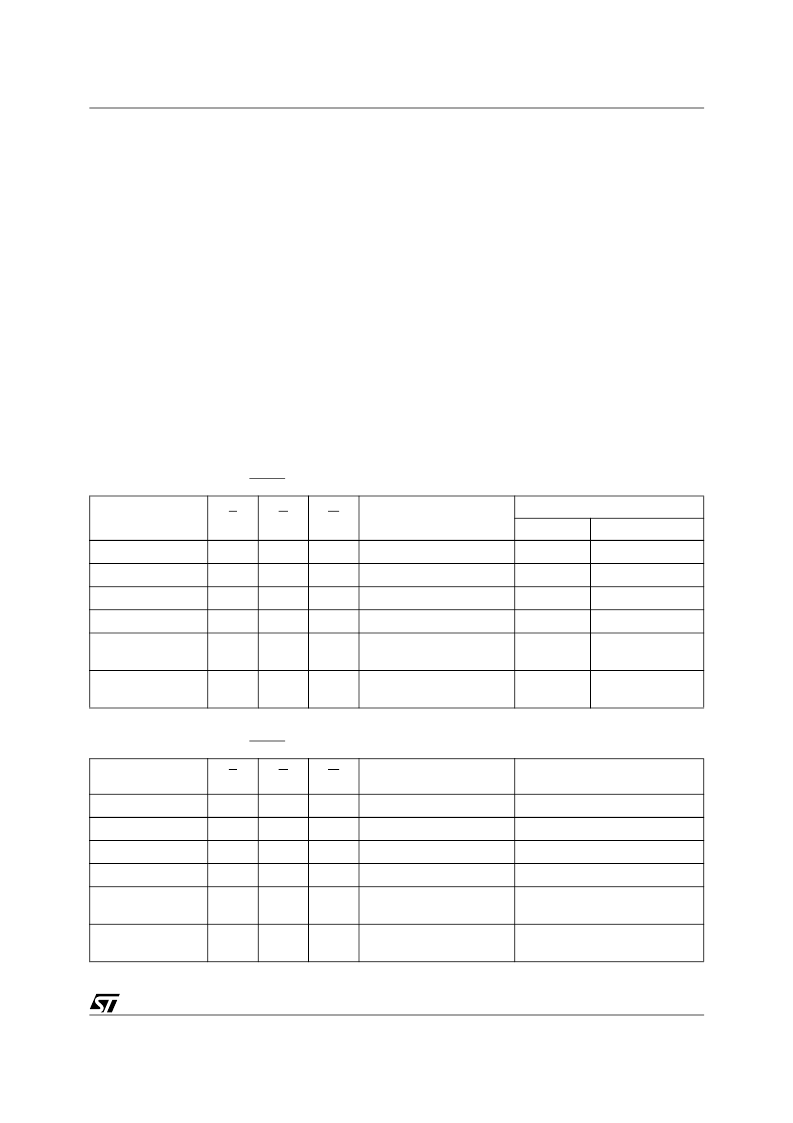
Table 5. Bus Operations, BYTE = V
IL
Note: X = V
IL
or V
IH
.
Table 6. Bus Operations, BYTE = V
IH
Note: X = V
IL
or V
IH
.
Operation
E
G
W
Address Inputs
DQ15A–1, A0-A16
Data Inputs/Outputs
DQ14-DQ8
DQ7-DQ0
Bus Read
V
IL
V
IL
V
IH
Cell Address
Hi-Z
Data Output
Bus Write
V
IL
V
IH
V
IL
Command Address
Hi-Z
Data Input
Output Disable
X
V
IH
V
IH
X
Hi-Z
Hi-Z
Standby
V
IH
X
X
X
Hi-Z
Hi-Z
Read Manufacturer
Code
V
IL
V
IL
V
IH
A0 = V
IL
, A1 = V
IL
, A9 = V
ID
,
Others V
IL
or V
IH
Hi-Z
20h
Read Device Code
V
IL
V
IL
V
IH
A0 = V
IH
, A1 = V
IL
, A9 = V
ID
,
Others V
IL
or V
IH
Hi-Z
51h (M29W200BT)
57h (M29W200BB)
Operation
E
G
W
Address Inputs
A0-A16
Data Inputs/Outputs
DQ15A–1, DQ14-DQ0
Bus Read
V
IL
V
IL
V
IH
Cell Address
Data Output
Bus Write
V
IL
V
IH
V
IL
Command Address
Data Input
Output Disable
X
V
IH
V
IH
X
Hi-Z
Standby
V
IH
X
X
X
Hi-Z
Read Manufacturer
Code
V
IL
V
IL
V
IH
A0 = V
IL
, A1 = V
IL
, A9 = V
ID
,
Others V
IL
or V
IH
0020h
Read Device Code
V
IL
V
IL
V
IH
A0 = V
IH
, A1 = V
IL
, A9 = V
ID
,
Others V
IL
or V
IH
0051h (M29W200BT)
0057h (M29W200BB)
BUS OPERATIONS
There are five standard bus operations that control
the device. These are Bus Read, Bus Write, Out-
put Disable, Standby and Automatic Standby. See
Tables 5 and 6, Bus Operations, for a summary.
Typically glitches of less than 5ns on Chip Enable
or Write Enable are ignored by the memory and do
not affect bus operations.
Bus Read.
Bus Read operations read from the
memory cells, or specific registers in the Com-
mand Interface. A valid Bus Read operation in-
volves setting the desired address on the Address
Inputs, applying a Low signal, V
IL
, to Chip Enable
and Output Enable and keeping Write Enable
High, V
IH
. The Data Inputs/Outputs will output the
value, see Figure 8, Read Mode AC Waveforms,
and Table 14, Read AC Characteristics, for details
of when the output becomes valid.
Bus Write.
Bus Write operations write to the
Command Interface. A valid Bus Write operation
begins by setting the desired address on the Ad-
dress Inputs. The Address Inputs are latched by
the Command Interface on the falling edge of Chip
Enable or Write Enable, whichever occurs last.
The Data Inputs/Outputs are latched by the Com-
mand Interface on the rising edge of Chip Enable
or Write Enable, whichever occurs first. Output En-
able must remain High, V
IH
, during the whole Bus
Write operation. See Figures 9 and 10, Write AC
Waveforms, and Tables 15 and 16, Write AC
Characteristics, for details of the timing require-
ments.
Output Disable.
The Data Inputs/Outputs are in
the high impedance state when Output Enable is
High, V
IH
.
Standby.
When Chip Enable is High, V
IH
, the
memory enters Standby mode and the Data In-
puts/Outputs pins are placed in the high-imped-
ance state. To reduce the Supply Current to the
Standby Supply Current, I
CC2
, Chip Enable should
be held within V
CC
± 0.2V. For the Standby current
level see Table 13, DC Characteristics.
During program or erase operations the memory
will continue to use the Program/Erase Supply
Current, I
CC3
, for Program or Erase operations un-
til the operation completes.
相关PDF资料 |
PDF描述 |
|---|---|
| M29W200BT120M6E | 2 Mbit (256Kb x8 or 128Kb x16, Boot Block) Low Voltage Single Supply Flash Memory |
| M29W200BT120M6F | 2 Mbit (256Kb x8 or 128Kb x16, Boot Block) Low Voltage Single Supply Flash Memory |
| M29W200BT120N1 | 2 Mbit (256Kb x8 or 128Kb x16, Boot Block) Low Voltage Single Supply Flash Memory |
| M29W200BT120N1E | 2 Mbit (256Kb x8 or 128Kb x16, Boot Block) Low Voltage Single Supply Flash Memory |
| M29W200BT120N1F | 2 Mbit (256Kb x8 or 128Kb x16, Boot Block) Low Voltage Single Supply Flash Memory |
相关代理商/技术参数 |
参数描述 |
|---|---|
| M29W200BT55N1 | 功能描述:闪存 256Kx8 or 128Kx16 55 RoHS:否 制造商:ON Semiconductor 数据总线宽度:1 bit 存储类型:Flash 存储容量:2 MB 结构:256 K x 8 定时类型: 接口类型:SPI 访问时间: 电源电压-最大:3.6 V 电源电压-最小:2.3 V 最大工作电流:15 mA 工作温度:- 40 C to + 85 C 安装风格:SMD/SMT 封装 / 箱体: 封装:Reel |
| M29W200BT70M1 | 功能描述:闪存 256Kx8 or 128Kx16 70 RoHS:否 制造商:ON Semiconductor 数据总线宽度:1 bit 存储类型:Flash 存储容量:2 MB 结构:256 K x 8 定时类型: 接口类型:SPI 访问时间: 电源电压-最大:3.6 V 电源电压-最小:2.3 V 最大工作电流:15 mA 工作温度:- 40 C to + 85 C 安装风格:SMD/SMT 封装 / 箱体: 封装:Reel |
| M29W200BT70N1 | 功能描述:闪存 256Kx8 or 128Kx16 70 RoHS:否 制造商:ON Semiconductor 数据总线宽度:1 bit 存储类型:Flash 存储容量:2 MB 结构:256 K x 8 定时类型: 接口类型:SPI 访问时间: 电源电压-最大:3.6 V 电源电压-最小:2.3 V 最大工作电流:15 mA 工作温度:- 40 C to + 85 C 安装风格:SMD/SMT 封装 / 箱体: 封装:Reel |
| M29W200BT70N6E | 功能描述:IC FLASH 2MBIT 70NS 48TSOP RoHS:是 类别:集成电路 (IC) >> 存储器 系列:- 标准包装:1,000 系列:- 格式 - 存储器:RAM 存储器类型:移动 SDRAM 存储容量:256M(8Mx32) 速度:133MHz 接口:并联 电源电压:1.7 V ~ 1.95 V 工作温度:-40°C ~ 85°C 封装/外壳:90-VFBGA 供应商设备封装:90-VFBGA(8x13) 包装:带卷 (TR) 其它名称:557-1327-2 |
| M29W200BT90N6 | 功能描述:闪存 256Kx8 or 128Kx16 90 RoHS:否 制造商:ON Semiconductor 数据总线宽度:1 bit 存储类型:Flash 存储容量:2 MB 结构:256 K x 8 定时类型: 接口类型:SPI 访问时间: 电源电压-最大:3.6 V 电源电压-最小:2.3 V 最大工作电流:15 mA 工作温度:- 40 C to + 85 C 安装风格:SMD/SMT 封装 / 箱体: 封装:Reel |
发布紧急采购,3分钟左右您将得到回复。