- 您现在的位置:买卖IC网 > PDF目录359053 > M29W800AT100ZA5T (意法半导体) 8 Mbit 1Mb x8 or 512Kb x16, Boot Block Low Voltage Single Supply Flash Memory PDF资料下载
参数资料
| 型号: | M29W800AT100ZA5T |
| 厂商: | 意法半导体 |
| 英文描述: | 8 Mbit 1Mb x8 or 512Kb x16, Boot Block Low Voltage Single Supply Flash Memory |
| 中文描述: | 8兆1兆x8或512KB的x16插槽,引导块低压单电源闪存 |
| 文件页数: | 3/33页 |
| 文件大小: | 234K |
| 代理商: | M29W800AT100ZA5T |
第1页第2页当前第3页第4页第5页第6页第7页第8页第9页第10页第11页第12页第13页第14页第15页第16页第17页第18页第19页第20页第21页第22页第23页第24页第25页第26页第27页第28页第29页第30页第31页第32页第33页
3/33
M29W800AT, M29W800AB
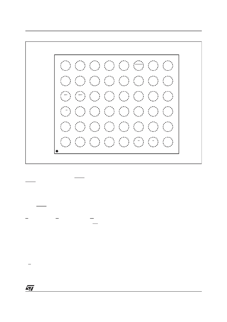
Figure 4. LFBGA Connections (Top view through package)
AI00656
D
E
F
8
7
6
5
4
3
2
1
B
C
A
VSS
DQ15
A–1
A15
A14
A12
A13
DQ3
DQ11
DQ10
A18
DU
RB
DQ1
DQ9
DQ8
DQ0
A6
A17
A7
G
E
A0
A4
A3
DQ2
DQ6
DQ13
DQ14
A10
A8
A9
DQ4
VCC
DQ12
DQ5
DU
DU
RP
W
A11
DQ7
A1
2
VSS
A5
DU
A16
BYTE
Memory Blocks
The devices featureasymmetrically blocked archi-
tecture providing system memoryintegration. Both
M29W800AT and M29W800AB devices have an
array of 19 blocks, one Boot Block of 16 KBytes or
8 KWords, two Parameter Blocks of 8 KBytes or 4
KWords, one Main Block of 32 KBytes or 16
KWords and fifteen Main Blocks of 64 KBytes or
32 KWords. The M29W800AT has the Boot Block
at the top of the memory address space and the
M29W800AB locates theBoot Block startingat the
bottom. The memory maps are showed in Figure
5.
Each block can be erased separately, any combi-
nation of blocks can be specified for multi-block
erase or the entirechip maybe erased. The Erase
operations are managed automatically by the P/
E.C. The block erase operation can be suspended
in order to read from or program to any block not
being erased, and then resumed.
Block protection provides additional data security.
Each block can be separately protected or unpro-
tected against Program or Erase on programming
equipment. All previously protected blocks can be
temporarily unprotected in the application.
Organisation
The M29W800A is organised as 1M x8 or 512K
x16 bits selectable by the BYTE signal. When
BYTE is Low the Byte-wide x8 organisation is se-
lected and the address lines are DQ15A–1 and
A0-A18. The Data Input/Output signal DQ15A–1
acts as address line A–1 which selects the lower
or upper Byte of the memory word for output on
DQ0-DQ7, DQ8-DQ14remain at High impedance.
When BYTE isHigh the memory uses the address
inputs A0-A18 and the Data Input/Outputs DQ0-
DQ15. Memorycontrol isprovided by Chip Enable
E, Output Enable G and Write Enable W inputs.
A Reset/Block Temporary Unprotection RP tri-lev-
el input provides a hardware reset when pulled
Low, and when held High (at V
ID
) temporarily un-
protects blocks previously protected allowing them
to be programed and erased. Erase and Program
operations are controlled by an internal Program/
Erase Controller (P/E.C.). Status Register data
output on DQ7 provides a Data Polling signal, and
DQ6 and DQ2 provide Toggle signals to indicate
the state of the P/E.C operations. A Ready/Busy
RB output indicates the completion of the internal
algorithms.
相关PDF资料 |
PDF描述 |
|---|---|
| M29W800AB90ZA5T | 8 Mbit 1Mb x8 or 512Kb x16, Boot Block Low Voltage Single Supply Flash Memory |
| M29W800AT90ZA5T | 8 Mbit 1Mb x8 or 512Kb x16, Boot Block Low Voltage Single Supply Flash Memory |
| M29W800AB80ZA5T | 8 Mbit 1Mb x8 or 512Kb x16, Boot Block Low Voltage Single Supply Flash Memory |
| M29W800AT80ZA5T | 8 Mbit 1Mb x8 or 512Kb x16, Boot Block Low Voltage Single Supply Flash Memory |
| M29W800AB90M6T | Circular Connector; No. of Contacts:12; Series:JT02R; Body Material:Aluminum; Connecting Termination:Crimp; Connector Shell Size:14; Circular Contact Gender:Pin; Circular Shell Style:Box Mount Receptacle; Insert Arrangement:14-97 |
相关代理商/技术参数 |
参数描述 |
|---|---|
| M29W800AT120M1 | 功能描述:闪存 1Mx8 or 512Kx16 120n RoHS:否 制造商:ON Semiconductor 数据总线宽度:1 bit 存储类型:Flash 存储容量:2 MB 结构:256 K x 8 定时类型: 接口类型:SPI 访问时间: 电源电压-最大:3.6 V 电源电压-最小:2.3 V 最大工作电流:15 mA 工作温度:- 40 C to + 85 C 安装风格:SMD/SMT 封装 / 箱体: 封装:Reel |
| M29W800AT120N1 | 功能描述:闪存 1Mx8 or 512Kx16 120n RoHS:否 制造商:ON Semiconductor 数据总线宽度:1 bit 存储类型:Flash 存储容量:2 MB 结构:256 K x 8 定时类型: 接口类型:SPI 访问时间: 电源电压-最大:3.6 V 电源电压-最小:2.3 V 最大工作电流:15 mA 工作温度:- 40 C to + 85 C 安装风格:SMD/SMT 封装 / 箱体: 封装:Reel |
| M29W800AT120N6 | 功能描述:闪存 STD FLASH RoHS:否 制造商:ON Semiconductor 数据总线宽度:1 bit 存储类型:Flash 存储容量:2 MB 结构:256 K x 8 定时类型: 接口类型:SPI 访问时间: 电源电压-最大:3.6 V 电源电压-最小:2.3 V 最大工作电流:15 mA 工作温度:- 40 C to + 85 C 安装风格:SMD/SMT 封装 / 箱体: 封装:Reel |
| M29W800AT120ZA6 | 功能描述:闪存 LFBGA48 1MX8 512KX16 RoHS:否 制造商:ON Semiconductor 数据总线宽度:1 bit 存储类型:Flash 存储容量:2 MB 结构:256 K x 8 定时类型: 接口类型:SPI 访问时间: 电源电压-最大:3.6 V 电源电压-最小:2.3 V 最大工作电流:15 mA 工作温度:- 40 C to + 85 C 安装风格:SMD/SMT 封装 / 箱体: 封装:Reel |
| M29W800AT80N1 | 功能描述:闪存 1Mx8 or 512Kx16 80ns RoHS:否 制造商:ON Semiconductor 数据总线宽度:1 bit 存储类型:Flash 存储容量:2 MB 结构:256 K x 8 定时类型: 接口类型:SPI 访问时间: 电源电压-最大:3.6 V 电源电压-最小:2.3 V 最大工作电流:15 mA 工作温度:- 40 C to + 85 C 安装风格:SMD/SMT 封装 / 箱体: 封装:Reel |
发布紧急采购,3分钟左右您将得到回复。