- 您现在的位置:买卖IC网 > PDF目录132980 > M30263M3A-XXXFP-U3 16-BIT, FLASH, 20 MHz, MICROCONTROLLER, PDSO42 PDF资料下载
参数资料
| 型号: | M30263M3A-XXXFP-U3 |
| 元件分类: | 微控制器/微处理器 |
| 英文描述: | 16-BIT, FLASH, 20 MHz, MICROCONTROLLER, PDSO42 |
| 封装: | 8.40 X 17.50 MM, 0.80 MM PITCH, LEAD FREE, PLASTIC, SSOP-42 |
| 文件页数: | 300/352页 |
| 文件大小: | 2423K |
| 代理商: | M30263M3A-XXXFP-U3 |
第1页第2页第3页第4页第5页第6页第7页第8页第9页第10页第11页第12页第13页第14页第15页第16页第17页第18页第19页第20页第21页第22页第23页第24页第25页第26页第27页第28页第29页第30页第31页第32页第33页第34页第35页第36页第37页第38页第39页第40页第41页第42页第43页第44页第45页第46页第47页第48页第49页第50页第51页第52页第53页第54页第55页第56页第57页第58页第59页第60页第61页第62页第63页第64页第65页第66页第67页第68页第69页第70页第71页第72页第73页第74页第75页第76页第77页第78页第79页第80页第81页第82页第83页第84页第85页第86页第87页第88页第89页第90页第91页第92页第93页第94页第95页第96页第97页第98页第99页第100页第101页第102页第103页第104页第105页第106页第107页第108页第109页第110页第111页第112页第113页第114页第115页第116页第117页第118页第119页第120页第121页第122页第123页第124页第125页第126页第127页第128页第129页第130页第131页第132页第133页第134页第135页第136页第137页第138页第139页第140页第141页第142页第143页第144页第145页第146页第147页第148页第149页第150页第151页第152页第153页第154页第155页第156页第157页第158页第159页第160页第161页第162页第163页第164页第165页第166页第167页第168页第169页第170页第171页第172页第173页第174页第175页第176页第177页第178页第179页第180页第181页第182页第183页第184页第185页第186页第187页第188页第189页第190页第191页第192页第193页第194页第195页第196页第197页第198页第199页第200页第201页第202页第203页第204页第205页第206页第207页第208页第209页第210页第211页第212页第213页第214页第215页第216页第217页第218页第219页第220页第221页第222页第223页第224页第225页第226页第227页第228页第229页第230页第231页第232页第233页第234页第235页第236页第237页第238页第239页第240页第241页第242页第243页第244页第245页第246页第247页第248页第249页第250页第251页第252页第253页第254页第255页第256页第257页第258页第259页第260页第261页第262页第263页第264页第265页第266页第267页第268页第269页第270页第271页第272页第273页第274页第275页第276页第277页第278页第279页第280页第281页第282页第283页第284页第285页第286页第287页第288页第289页第290页第291页第292页第293页第294页第295页第296页第297页第298页第299页当前第300页第301页第302页第303页第304页第305页第306页第307页第308页第309页第310页第311页第312页第313页第314页第315页第316页第317页第318页第319页第320页第321页第322页第323页第324页第325页第326页第327页第328页第329页第330页第331页第332页第333页第334页第335页第336页第337页第338页第339页第340页第341页第342页第343页第344页第345页第346页第347页第348页第349页第350页第351页第352页
7. Clock Generation Circuit
page 37
8
2
3
f
o
5
0
2
,
5
1
.
r
a
M
0
.
1
.
v
e
R
0
1
0
-
2
0
2
0
B
9
0
J
E
R
)
T
6
2
/
C
6
1
M
,
A
6
2
/
C
6
1
M
(
p
u
o
r
G
A
6
2
/
C
6
1
M
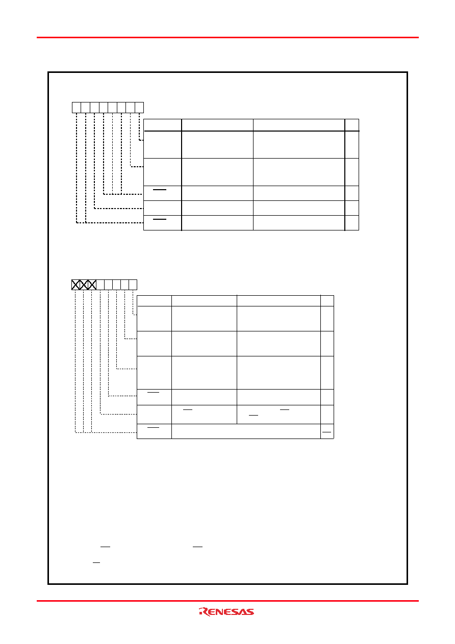
Figure 7.6. PCLKR Register and PM2 Register
Function
Bit symbol
Bit name
Peripheral clock select register (Note)
Symbol
Address
When reset
PCLKR
025E16
000000112
RW
b7
b6
b5
b4
b3
b2
b1
b0
PCLK0
Timers A, B clock select bit
(Clock source for the
timers A, B, and the dead
timer)
0 : f2
1 : f1
00 0
Reserved bit
Must set to
“0”
Note: Write to this register after setting the PRC0 bit in the PRCR register to “1” (write enable).
00
PCLK1
SI/O clock select bit
(Clock source for UART0
to UART2)
0 : f2SIO
1 : f1SIO
RW
(b4-b2)
Reserved bit
Must set to
“0”
RW
(b7-b6)
RW
PCLK5
Clock output function
expansion select bit
Refer to Table 7.5.3.1 Function
of CLKOUT pin
Function
Bit symbol
Bit name
Processeor mode register 2 (Note 1)
Symbol
Address
When reset
PM2
001E16
XXX000002
RW
b7
b6
b5
b4
b3
b2
b1
b0
PM20
Specifying Wait when
Accessing SFR at PLL
Operation
0 : 2 wait
1 : 1 wait
0
Nothing is assigned. When write, set to “0”. When read,
its content is indeterminate.
PM21
System clock protective bit
0 : Clock is protected by PRCR
register
1 : Clock modification disabled
RW
(b7-b5)
PM22
PM24
(b3)
WDT count source
protective bit
Reserved bit
0 : CPU clock is used for the
watchdog timer count source
1 : On-chip oscillator clock is used
for the watchdog timer count
source
Must set to “0”
P85/NMI configuration bit
RW
(Note 2)
(Note 3,4)
(Note 3,5)
(Note 6,7)
Note 1: Write to this register after setting the PRC1 bit in the PRCR register to “1” (write enable).
Note 2: This bit can only be rewritten while the PLC07 bit is “0” (PLL turned off). Also, set the PM20 bit to “0” (2 wait)
when PLL clock > 16MHz. Note that if the clock source for the CPU clock is to be changed from PLL clock
to another, the PLC07 bit must be set to "0" before setting the PM20 bit.
Note 3: Once this bit is set to “1”, it cannot be cleared to “0” in a program.
Note 4: If the PM21 bit is set to “1”, writing to the following bits has no efftect:
CM02 bit in the CM0 register
CM05 bit in the CM0 register (main clock is not halted)
CM07 bit in the CM0 register (CPU clock source does not change)
CM10 bit in the CM1 register (stop mode is not entered)
CM11 bit in the CM1 register (CPU clock source does not change)
CM20 bit in the CM2 register (oscillation stop, re-oscillation detection function settings do not change)
All bits in the PLC0 register (PLL frequency synthesizer setting do not change)
Be aware that the WAIT instruction cannot be executed when the PM21 bit is set to "1".
Note 5: Setting the PM22 bit to “1” results in the following conditions:
The on-chip oscillator starts oscillating, and the on-chip oscillator clock becomes the watchdog timer count
source.
The CM10 bit in the CM1 register is disabled against write. (Writing a “1” has no effect, nor is stop mode
entered.)
The watchdog timer does not stop when in wait mode.
Note 6: For NMI function, the PM24 bit must be set to “1”(NMI function) in first instruction after rest. Once this bit is
set to “1”, it cannot be cleared to “0” in a program. When the PM24 bit is set to “1”, the P85 direction register
must be “0”(input mode).
Note 7: SD input is valid regardless of the PM24 setting.
0 : P85 function (NMI disable)
1 : NMI function
相关PDF资料 |
PDF描述 |
|---|---|
| M37545G4-XXXGP | 8-BIT, MROM, 4 MHz, MICROCONTROLLER, PQFP32 |
| M37545G4KP | 8-BIT, MROM, 4 MHz, MICROCONTROLLER, PDSO32 |
| M37546G4SP | 8-BIT, MROM, 8 MHz, MICROCONTROLLER, PDIP32 |
| M30201F6FP | 16-BIT, FLASH, 10 MHz, MICROCONTROLLER, PQFP56 |
| M30201F6TFP | 16-BIT, FLASH, 10 MHz, MICROCONTROLLER, PQFP56 |
相关代理商/技术参数 |
参数描述 |
|---|---|
| M30263T2-CPE-FP | 制造商:Renesas Electronics Corporation 功能描述:DEV COMPACT EMULATOR - Bulk |
| M30263T-EPB-FP | 制造商:Renesas Electronics Corporation 功能描述:DEV EMULATOR ACCESSORY - Bulk |
| M30280F6HP | 制造商:Renesas Electronics Corporation 功能描述:IC,microcontroller,M16C/Tiny,1 |
| M30280F6HP D3 | 制造商:Renesas Electronics Corporation 功能描述: |
| M30280F6HP D5 | 制造商:Renesas Electronics Corporation 功能描述: |
发布紧急采购,3分钟左右您将得到回复。