- 您现在的位置:买卖IC网 > PDF目录45021 > M30620SPGP 16-BIT, 24 MHz, MICROCONTROLLER, PQFP100 PDF资料下载
参数资料
| 型号: | M30620SPGP |
| 元件分类: | 微控制器/微处理器 |
| 英文描述: | 16-BIT, 24 MHz, MICROCONTROLLER, PQFP100 |
| 封装: | 14 X 14 MM, 0.50 MM PITCH, PLASTIC, LQFP-100 |
| 文件页数: | 25/104页 |
| 文件大小: | 1313K |
| 代理商: | M30620SPGP |
第1页第2页第3页第4页第5页第6页第7页第8页第9页第10页第11页第12页第13页第14页第15页第16页第17页第18页第19页第20页第21页第22页第23页第24页当前第25页第26页第27页第28页第29页第30页第31页第32页第33页第34页第35页第36页第37页第38页第39页第40页第41页第42页第43页第44页第45页第46页第47页第48页第49页第50页第51页第52页第53页第54页第55页第56页第57页第58页第59页第60页第61页第62页第63页第64页第65页第66页第67页第68页第69页第70页第71页第72页第73页第74页第75页第76页第77页第78页第79页第80页第81页第82页第83页第84页第85页第86页第87页第88页第89页第90页第91页第92页第93页第94页第95页第96页第97页第98页第99页第100页第101页第102页第103页第104页
1. Overview
Page 25 of 96
1.6
Pin Description
I : Input
O : Output
I/O : Input and output
Power Supply : Power supplies which relate to the external bus pins are separated as VCC2, thus they can be
interfaced using the different voltage as VCC1.
NOTES:
1. In this manual, hereafter, VCC refers to VCC1 unless otherwise noted.
2. In M16C/62PT, apply 4.0 to 5.5 V to the VCC1 and VCC2 pins. Also the apply condition is that VCC1 = VCC2.
3. When use VCC1 > VCC2, contacts due to some points or restrictions to be checked.
4. Bus control pins in M16C/62PT cannot be used.
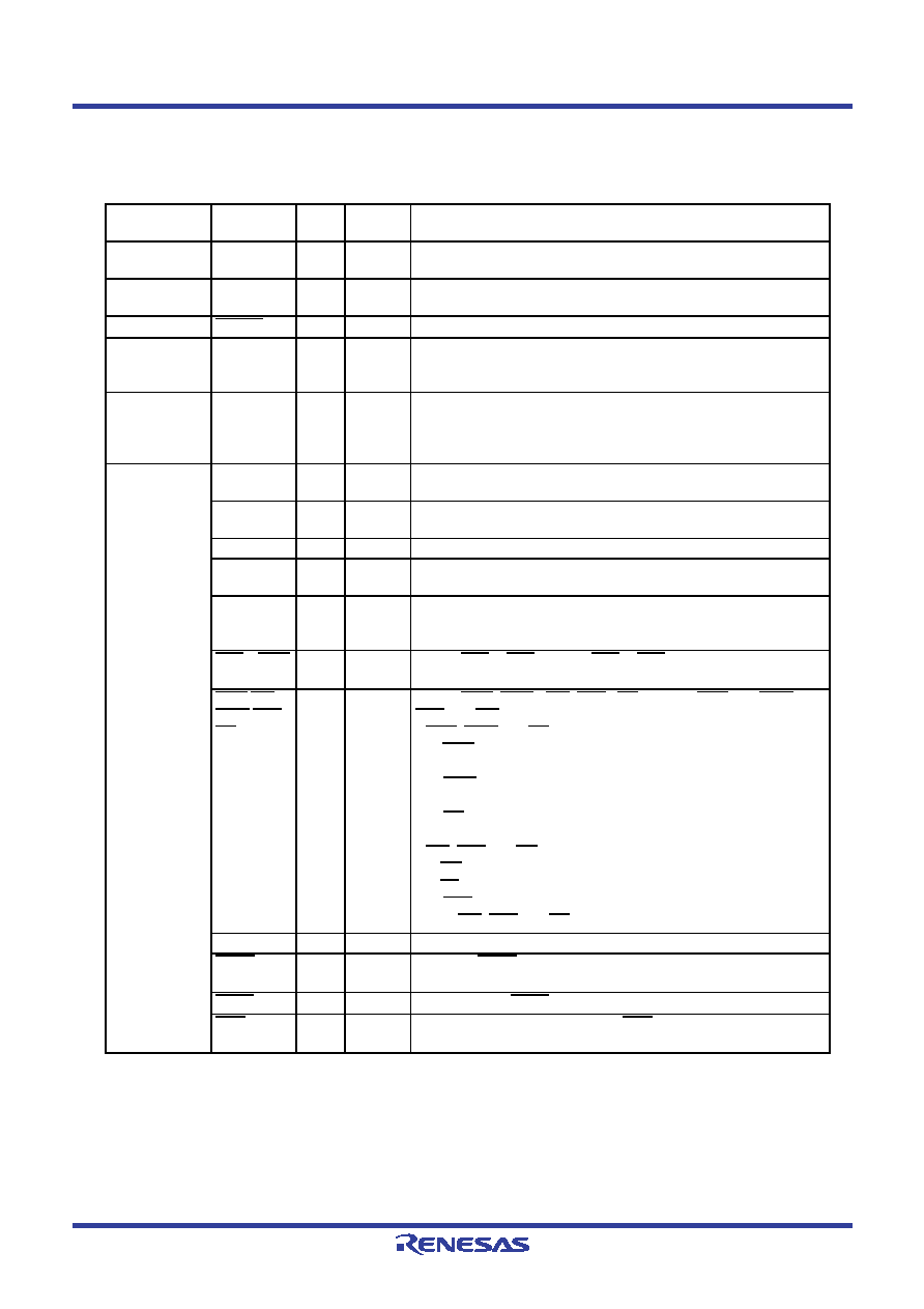
Table 1.17
Pin Description (100-pin and 128-pin Version) (1)
Signal Name
Pin Name
I/O
Type
Power
Supply(3)
Description
Power supply
input
VCC1,VCC2
VSS
I
Apply 2.7 to 5.5 V to the VCC1 and VCC2 pins and 0 V to the VSS
pin. The VCC apply condition is that VCC1
≥ VCC2. (1, 2)
Analog power
supply input
AVCC
AVSS
I
VCC1
Applies the power supply for the A/D converter. Connect the AVCC
pin to VCC1. Connect the AVSS pin to VSS.
Reset input
RESET
IVCC1
The microcomputer is in a reset state when applying “L” to the this pin.
CNVSS
I
VCC1
Switches processor mode. Connect this pin to VSS to when after
a reset to start up in single-chip mode. Connect this pin to VCC1 to
start up in microprocessor mode.
External data
bus width
select input
BYTE
I
VCC1
Switches the data bus in external memory space. The data bus is
16 bits long when the this pin is held "L" and 8 bits long when the
this pin is held "H". Set it to either one. Connect this pin to VSS
when an single-chip mode.
Bus control
pins (4)
D0 to D7
I/O
VCC2
Inputs and outputs data (D0 to D7) when these pins are set as the
separate bus.
D8 to D15
I/O
VCC2
Inputs and outputs data (D8 to D15) when external 16-bit data bus
is set as the separate bus.
A0 to A19
O
VCC2
Output address bits (A0 to A19).
A0/D0 to
A7/D7
I/O
VCC2
Input and output data (D0 to D7) and output address bits (A0 to A7) by
timesharing when external 8-bit data bus are set as the multiplexed bus.
A1/D0 to
A8/D7
I/O
VCC2
Input and output data (D0 to D7) and output address bits (A1 to A8)
by timesharing when external 16-bit data bus are set as the
multiplexed bus.
CS0 to CS3
O
VCC2
Output CS0 to CS3 signals. CS0 to CS3 are chip-select signals to
specify an external space.
WRL/WR
WRH/BHE
RD
O
VCC2
Output WRL, WRH, (WR, BHE), RD signals. WRL and WRH or
BHE and WR can be switched by program.
WRL, WRH and RD are selected
The WRL signal becomes "L" by writing data to an even address in
an external memory space.
The WRH signal becomes "L" by writing data to an odd address in
an external memory space.
The RD pin signal becomes "L" by reading data in an external
memory space.
WR, BHE and RD are selected
The WR signal becomes "L" by writing data in an external memory space.
The RD signal becomes "L" by reading data in an external memory space.
The BHE signal becomes "L" by accessing an odd address.
Select WR, BHE and RD for an external 8-bit data bus.
ALE
O
VCC2
ALE is a signal to latch the address.
HOLD
I
VCC2
While the HOLD pin is held "L", the microcomputer is placed in a
hold state.
HLDA
O
VCC2
In a hold state, HLDA outputs a "L" signal.
RDY
I
VCC2
While applying a "L" signal to the RDY pin, the microcomputer is
placed in a wait state.
相关PDF资料 |
PDF描述 |
|---|---|
| M3062AMCT-XXXFP | 16-BIT, MROM, 24 MHz, MICROCONTROLLER, PQFP100 |
| M30624FGPGP | 16-BIT, FLASH, 24 MHz, MICROCONTROLLER, PQFP100 |
| M30626MWP-XXXGP | 16-BIT, MROM, 24 MHz, MICROCONTROLLER, PQFP100 |
| M30624MWP-XXXGP | 16-BIT, MROM, 24 MHz, MICROCONTROLLER, PQFP100 |
| M30622F8PFP | 16-BIT, FLASH, 24 MHz, MICROCONTROLLER, PQFP100 |
相关代理商/技术参数 |
参数描述 |
|---|---|
| M30620SPGP D3 | 制造商:Renesas Electronics Corporation 功能描述: |
| M30620SPGP#U3 | 制造商:Renesas Electronics Corporation 功能描述: |
| M30620SPGP#U3C | 功能描述:IC M16C MCU ROMLESS 100LQFP RoHS:是 类别:集成电路 (IC) >> 嵌入式 - 微控制器, 系列:M16C™ M16C/60/62P 标准包装:96 系列:PIC® 16F 核心处理器:PIC 芯体尺寸:8-位 速度:20MHz 连通性:I²C,SPI 外围设备:欠压检测/复位,POR,PWM,WDT 输入/输出数:11 程序存储器容量:3.5KB(2K x 14) 程序存储器类型:闪存 EEPROM 大小:- RAM 容量:128 x 8 电压 - 电源 (Vcc/Vdd):2.3 V ~ 5.5 V 数据转换器:A/D 8x10b 振荡器型:内部 工作温度:-40°C ~ 125°C 封装/外壳:14-TSSOP(0.173",4.40mm 宽) 包装:管件 |
| M30620SPGP#U5 | 制造商:Renesas Electronics Corporation 功能描述: 制造商:Renesas Electronics Corporation 功能描述:16BIT MCU ROMLESS 30620 LQFP100 |
| M30620SPGP#U5C | 功能描述:IC M16C MCU ROMLESS 100LQFP RoHS:是 类别:集成电路 (IC) >> 嵌入式 - 微控制器, 系列:M16C™ M16C/60/62P 产品培训模块:CAN Basics Part-1 CAN Basics Part-2 Electromagnetic Noise Reduction Techniques Part 1 M16C Product Overview Part 1 M16C Product Overview Part 2 标准包装:1 系列:M16C™ M32C/80/87 核心处理器:M32C/80 芯体尺寸:16/32-位 速度:32MHz 连通性:EBI/EMI,I²C,IEBus,IrDA,SIO,UART/USART 外围设备:DMA,POR,PWM,WDT 输入/输出数:121 程序存储器容量:384KB(384K x 8) 程序存储器类型:闪存 EEPROM 大小:- RAM 容量:24K x 8 电压 - 电源 (Vcc/Vdd):3 V ~ 5.5 V 数据转换器:A/D 34x10b,D/A 2x8b 振荡器型:内部 工作温度:-20°C ~ 85°C 封装/外壳:144-LQFP 包装:托盘 产品目录页面:749 (CN2011-ZH PDF) 配用:R0K330879S001BE-ND - KIT DEV RSK M32C/87 |
发布紧急采购,3分钟左右您将得到回复。