- 您现在的位置:买卖IC网 > PDF目录45021 > M30620SPGP 16-BIT, 24 MHz, MICROCONTROLLER, PQFP100 PDF资料下载
参数资料
| 型号: | M30620SPGP |
| 元件分类: | 微控制器/微处理器 |
| 英文描述: | 16-BIT, 24 MHz, MICROCONTROLLER, PQFP100 |
| 封装: | 14 X 14 MM, 0.50 MM PITCH, PLASTIC, LQFP-100 |
| 文件页数: | 77/104页 |
| 文件大小: | 1313K |
| 代理商: | M30620SPGP |
第1页第2页第3页第4页第5页第6页第7页第8页第9页第10页第11页第12页第13页第14页第15页第16页第17页第18页第19页第20页第21页第22页第23页第24页第25页第26页第27页第28页第29页第30页第31页第32页第33页第34页第35页第36页第37页第38页第39页第40页第41页第42页第43页第44页第45页第46页第47页第48页第49页第50页第51页第52页第53页第54页第55页第56页第57页第58页第59页第60页第61页第62页第63页第64页第65页第66页第67页第68页第69页第70页第71页第72页第73页第74页第75页第76页当前第77页第78页第79页第80页第81页第82页第83页第84页第85页第86页第87页第88页第89页第90页第91页第92页第93页第94页第95页第96页第97页第98页第99页第100页第101页第102页第103页第104页
5. Electrical Characteristics
Rev.2.41
Jan 10, 2006
Page 72 of 96
REJ03B0001-0241
VCC1=VCC2=3V
Switching Characteristics
(VCC1 = VCC2 = 5V, VSS = 0V, at Topr =
20 to 85°C / 40 to 85°C unless otherwise specified)
NOTES:
1.
Calculated according to the BCLK frequency as follows:
2.
Calculated according to the BCLK frequency as follows:
n is “2” for 2-wait setting, “3” for 3-wait setting.
3.
Calculated according to the BCLK frequency as follows:
4.
Calculated according to the BCLK frequency as follows:
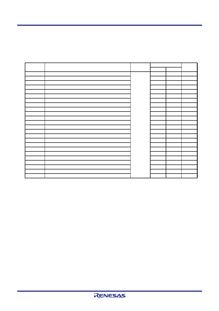
Table 5.48
Memory Expansion and Microprocessor Modes (for 2- to 3-wait setting, external area
access and multiplex bus selection)
Symbol
Parameter
Standard
Unit
Min.
Max.
td(BCLK-AD)
Address Output Delay Time
See
50
ns
th(BCLK-AD)
Address Output Hold Time (in relation to BCLK)
4
ns
th(RD-AD)
Address Output Hold Time (in relation to RD)
ns
th(WR-AD)
Address Output Hold Time (in relation to WR)
ns
td(BCLK-CS)
Chip Select Output Delay Time
50
ns
th(BCLK-CS)
Chip Select Output Hold Time (in relation to BCLK)
4
ns
th(RD-CS)
Chip Select Output Hold Time (in relation to RD)
ns
th(WR-CS)
Chip Select Output Hold Time (in relation to WR)
ns
td(BCLK-RD)
RD Signal Output Delay Time
40
ns
th(BCLK-RD)
RD Signal Output Hold Time
0
ns
td(BCLK-WR)
WR Signal Output Delay Time
40
ns
th(BCLK-WR)
WR Signal Output Hold Time
0
ns
td(BCLK-DB)
Data Output Delay Time (in relation to BCLK)
50
ns
th(BCLK-DB)
Data Output Hold Time (in relation to BCLK)
4
ns
td(DB-WR)
Data Output Delay Time (in relation to WR)
ns
th(WR-DB)
Data Output Hold Time (in relation to WR)
ns
td(BCLK-HLDA)
HLDA Output Delay Time
40
ns
td(BCLK-ALE)
ALE Signal Output Delay Time (in relation to BCLK)
25
ns
th(BCLK-ALE)
ALE Signal Output Hold Time (in relation to BCLK)
4ns
td(AD-ALE)
ALE Signal Output Delay Time (in relation to Address)
ns
th(AD-ALE)
ALE Signal Output Hold Time (in relation to Address)
ns
td(AD-RD)
RD Signal Output Delay From the End of Address
0
ns
td(AD-WR)
WR Signal Output Delay From the End of Address
0
ns
tdz(RD-AD)
Address Output Floating Start Time
8
ns
0.5x10
9
fBCLK
()
------------------------10 ns
[]
–
0.5x10
9
fBCLK
()
------------------------
50 ns
[]
–
0.5x10
9
fBCLK
()
------------------------
40 ns
[]
–
0.5x10
9
fBCLK
()
------------------------15 ns
[]
–
相关PDF资料 |
PDF描述 |
|---|---|
| M3062AMCT-XXXFP | 16-BIT, MROM, 24 MHz, MICROCONTROLLER, PQFP100 |
| M30624FGPGP | 16-BIT, FLASH, 24 MHz, MICROCONTROLLER, PQFP100 |
| M30626MWP-XXXGP | 16-BIT, MROM, 24 MHz, MICROCONTROLLER, PQFP100 |
| M30624MWP-XXXGP | 16-BIT, MROM, 24 MHz, MICROCONTROLLER, PQFP100 |
| M30622F8PFP | 16-BIT, FLASH, 24 MHz, MICROCONTROLLER, PQFP100 |
相关代理商/技术参数 |
参数描述 |
|---|---|
| M30620SPGP D3 | 制造商:Renesas Electronics Corporation 功能描述: |
| M30620SPGP#U3 | 制造商:Renesas Electronics Corporation 功能描述: |
| M30620SPGP#U3C | 功能描述:IC M16C MCU ROMLESS 100LQFP RoHS:是 类别:集成电路 (IC) >> 嵌入式 - 微控制器, 系列:M16C™ M16C/60/62P 标准包装:96 系列:PIC® 16F 核心处理器:PIC 芯体尺寸:8-位 速度:20MHz 连通性:I²C,SPI 外围设备:欠压检测/复位,POR,PWM,WDT 输入/输出数:11 程序存储器容量:3.5KB(2K x 14) 程序存储器类型:闪存 EEPROM 大小:- RAM 容量:128 x 8 电压 - 电源 (Vcc/Vdd):2.3 V ~ 5.5 V 数据转换器:A/D 8x10b 振荡器型:内部 工作温度:-40°C ~ 125°C 封装/外壳:14-TSSOP(0.173",4.40mm 宽) 包装:管件 |
| M30620SPGP#U5 | 制造商:Renesas Electronics Corporation 功能描述: 制造商:Renesas Electronics Corporation 功能描述:16BIT MCU ROMLESS 30620 LQFP100 |
| M30620SPGP#U5C | 功能描述:IC M16C MCU ROMLESS 100LQFP RoHS:是 类别:集成电路 (IC) >> 嵌入式 - 微控制器, 系列:M16C™ M16C/60/62P 产品培训模块:CAN Basics Part-1 CAN Basics Part-2 Electromagnetic Noise Reduction Techniques Part 1 M16C Product Overview Part 1 M16C Product Overview Part 2 标准包装:1 系列:M16C™ M32C/80/87 核心处理器:M32C/80 芯体尺寸:16/32-位 速度:32MHz 连通性:EBI/EMI,I²C,IEBus,IrDA,SIO,UART/USART 外围设备:DMA,POR,PWM,WDT 输入/输出数:121 程序存储器容量:384KB(384K x 8) 程序存储器类型:闪存 EEPROM 大小:- RAM 容量:24K x 8 电压 - 电源 (Vcc/Vdd):3 V ~ 5.5 V 数据转换器:A/D 34x10b,D/A 2x8b 振荡器型:内部 工作温度:-20°C ~ 85°C 封装/外壳:144-LQFP 包装:托盘 产品目录页面:749 (CN2011-ZH PDF) 配用:R0K330879S001BE-ND - KIT DEV RSK M32C/87 |
发布紧急采购,3分钟左右您将得到回复。