- 您现在的位置:买卖IC网 > PDF目录68607 > M30621MCN-XXXGP 16-BIT, MROM, 16 MHz, MICROCONTROLLER, PQFP80 PDF资料下载
参数资料
| 型号: | M30621MCN-XXXGP |
| 元件分类: | 微控制器/微处理器 |
| 英文描述: | 16-BIT, MROM, 16 MHz, MICROCONTROLLER, PQFP80 |
| 封装: | 14 X 14 MM, 0.65 MM PITCH, PLASTIC, QFP-80 |
| 文件页数: | 71/212页 |
| 文件大小: | 2676K |
| 代理商: | M30621MCN-XXXGP |
第1页第2页第3页第4页第5页第6页第7页第8页第9页第10页第11页第12页第13页第14页第15页第16页第17页第18页第19页第20页第21页第22页第23页第24页第25页第26页第27页第28页第29页第30页第31页第32页第33页第34页第35页第36页第37页第38页第39页第40页第41页第42页第43页第44页第45页第46页第47页第48页第49页第50页第51页第52页第53页第54页第55页第56页第57页第58页第59页第60页第61页第62页第63页第64页第65页第66页第67页第68页第69页第70页当前第71页第72页第73页第74页第75页第76页第77页第78页第79页第80页第81页第82页第83页第84页第85页第86页第87页第88页第89页第90页第91页第92页第93页第94页第95页第96页第97页第98页第99页第100页第101页第102页第103页第104页第105页第106页第107页第108页第109页第110页第111页第112页第113页第114页第115页第116页第117页第118页第119页第120页第121页第122页第123页第124页第125页第126页第127页第128页第129页第130页第131页第132页第133页第134页第135页第136页第137页第138页第139页第140页第141页第142页第143页第144页第145页第146页第147页第148页第149页第150页第151页第152页第153页第154页第155页第156页第157页第158页第159页第160页第161页第162页第163页第164页第165页第166页第167页第168页第169页第170页第171页第172页第173页第174页第175页第176页第177页第178页第179页第180页第181页第182页第183页第184页第185页第186页第187页第188页第189页第190页第191页第192页第193页第194页第195页第196页第197页第198页第199页第200页第201页第202页第203页第204页第205页第206页第207页第208页第209页第210页第211页第212页
CPU Rewrite Mode (Flash Memory Version)
162
Mitsubishi microcomputers
M16C / 62N Group (80-pin)
SINGLE-CHIP 16-BIT CMOS MICROCOMPUTER
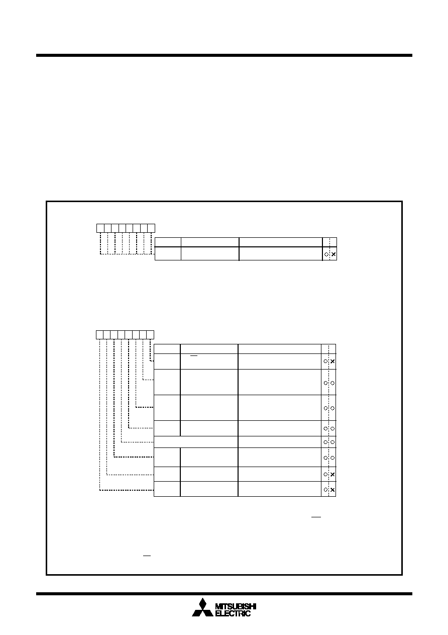
Flash memory control register 0
Symbol
Address
When reset
FMR0
03B716
XX0000012
W
R
b7
b6
b5
b4
b3
b2 b1
b0
FMR00
Bit symbol
Bit name
Function
RW
0: Busy (being written or erased)
1: Ready
CPU rewrite mode
select bit (Note 1)
0: Normal mode
(Software commands invalid)
1: CPU rewrite mode
(Software commands acceptable)
FMR01
0: Boot ROM area is accessed
1: User ROM area is accessed
Lock bit disable
select bit (Note 2)
0: Block lock by lock bit data is
enabled
1: Block lock by lock bit data is
disabled
Flash memory reset bit
(Note 3)
0: Normal operation
1: Reset
User ROM area select bit
(Note 4) (Effective in only
boot mode)
FMR02
FMR03
FMR05
0
Note 1: For this bit to be set to “1”, the user needs to write a “0” and then a “1” to it in succession.
When it is not this procedure, it is not enacted in “1”. This is necessary to ensure that no
interrupt or DMA transfer will be executed during the interval. Write to this bit only when
executing out of an area other than the internal flash memory. Also only when NMI pin is
“H” level. Clear this bit to “0” after read array command.
Note 2: For this bit to be set to “1”, the user needs to write a “0” and then a “1” to it in succession
when the CPU rewrite mode select bit = “1”. When it is not this procedure, it is not
enacted in “1”. This is necessary to ensure that no interrupt or DMA transfer will be
executed during the interval.
Note 3: Effective only when the CPU rewrite mode select bit = 1. After write “1”, write “0” when
RY/BY status flag is “1”.
Note 4: Write to this bit only when executing out of an area other than the internal flash memory.
RY/BY status flag
Reserved bit
Must always be set to “0”
Flash identification register
Symbol
Address
When reset
FIDR
03B416
0016
W
R
b7 b6
b5
b4
b3
b2
b1 b0
FIDR0
Bit symbol
Bit name
Function
RW
Flash value output
HND: 0016
Flash identification value
Procedure
(1) Write FF16 to the address 03B416
(2) Read address 03B416
Read value = FF16 DINOR flash memory
Read value = 0016 HND flash memory
0: Pass
1: Error
Program status flag
FMR06
0: Pass
1: Error
Erase status flag
FMR07
Figure 1.29.1. Flash identification register and flash memory control register 0
Bit 5 of the flash memory control register 0 is a user ROM area select bit which is effective in only boot
mode. If this bit is set to “1” in boot mode, the area to be accessed is switched from the boot ROM area to
the user ROM area. When the CPU rewrite mode needs to be used in boot mode, set this bit to “1”. Note
that if the microcomputer is booted from the user ROM area, it is always the user ROM area that can be
accessed and this bit has no effect. When in boot mode, the function of this bit is effective regardless of
whether the CPU rewrite mode is on or off. Write to this bit only when executing out of an area other than
the internal flash memory.
Bit 6 of the flash memory control register 0 is the program status flag used exclusively to read the operating
status of the auto program operation. If a program error occurs, it is set to “1”. Otherwise, it is “0”.
Bit 7 of the flash memory control register 0 is the erase status flag used exclusively to read the operating
status of the auto erase operation. If an erase error occurs, it is set to “1”. Otherwise, it is “0”.
相关PDF资料 |
PDF描述 |
|---|---|
| M30625FGNGP | 16-BIT, FLASH, 16 MHz, MICROCONTROLLER, PQFP80 |
| M306K7F8LRP | 16-BIT, FLASH, 8 MHz, MICROCONTROLLER, PQFP144 |
| M35052-001FP | 24 X 10 CHARACTERS CRT CHAR DSPL CTLR, PDSO20 |
| MAX6826LUT+T | Dual, Ultra-Low-Voltage SOT23 µP Supervisors with Manual Reset and Watchdog Timer |
| MAX6826MUT+T | Dual, Ultra-Low-Voltage SOT23 µP Supervisors with Manual Reset and Watchdog Timer |
相关代理商/技术参数 |
参数描述 |
|---|---|
| M30621MCP | 制造商:RENESAS 制造商全称:Renesas Technology Corp 功能描述:SINGLE-CHIP 16-BIT CMOS MICROCOMPUTER |
| M30621MCP-XXXGP | 制造商:RENESAS 制造商全称:Renesas Technology Corp 功能描述:SINGLE-CHIP 16-BIT CMOS MICROCOMPUTER |
| M30621MC-XXXGP | 制造商:RENESAS 制造商全称:Renesas Technology Corp 功能描述:SINGLE-CHIP 16-BIT CMOS MICROCOMPUTER |
| M30622 | 制造商:MITSUBISHI 制造商全称:Mitsubishi Electric Semiconductor 功能描述:SINGLE-CHIP 16-BIT CMOS MICROCOMPUTER |
| M30622E4-XXXFP | 制造商:RENESAS 制造商全称:Renesas Technology Corp 功能描述:16-BIT SINGLE-CHIP MICROCOMPUTER M16C FAMILY |
发布紧急采购,3分钟左右您将得到回复。